Transverse p-n-n microcavity-structured Ge light-emitting device and preparation method thereof

A p-n-n, light-emitting device technology, applied in the direction of semiconductor devices, electrical components, circuits, etc., can solve the problems of high technical level requirements, poor thermal stability, increase of non-radiative recombination centers, etc., to achieve simple process preparation, superior luminous performance, enhanced The effect of luminous efficiency

Pending Publication Date: 2018-05-29
FUJIAN UNIV OF TECH
View PDF6 Cites 3 Cited by
  • Summary
  • Abstract
  • Description
  • Claims
  • Application Information

AI Technical Summary

Problems solved by technology

The main research directions for Si-based III-V hybrid integrated lasers can be summarized into three types: First, the mature III-V semiconductor laser devices are packaged on Si-based chips by flip-chip welding technology. Although this method can ensure that the laser has Good performance, but the technical level is high, and the current technical level is not enough for mass production
Second, the mature III-V semiconductor laser device is pasted on the Si-based chip by bonding technology. This method has poor thermal stability and is not compatible with the silicon CMOS process, and the production cost is too high.
Third, by designing a suitable active layer and using the method of heteroepitaxy, directly epitaxial III-V group direct bandgap luminescent materials on Si substrates, due to the lattice mismatch between Si and III-V materials, epitaxy is difficult Relatively large, and the performance of the laser device prepared by this method needs to be improved
Since the lattice mismatch between Si and Ge is as high as 4.2%, when epitaxial Ge material on Si substrate, too many defects are inevitably introduced at the interface between Si and Ge, which not only increases the non-radiative recombination center, but also reduces the leakage current of the device. Increased; In addition, the direction of the light output of this vertical structure device is consistent with the direction of the current, and the light generated by it will also be absorbed by the metal electrode when it passes near the metal electrode, which further reduces the direct band luminous efficiency of Ge

Method used


Image

  • Transverse p-n-n microcavity-structured Ge light-emitting device and preparation method thereof

Examples


Embodiment Construction

[0026] The technical solutions in the embodiments of the present invention will be clearly and completely described below in conjunction with the accompanying drawings.

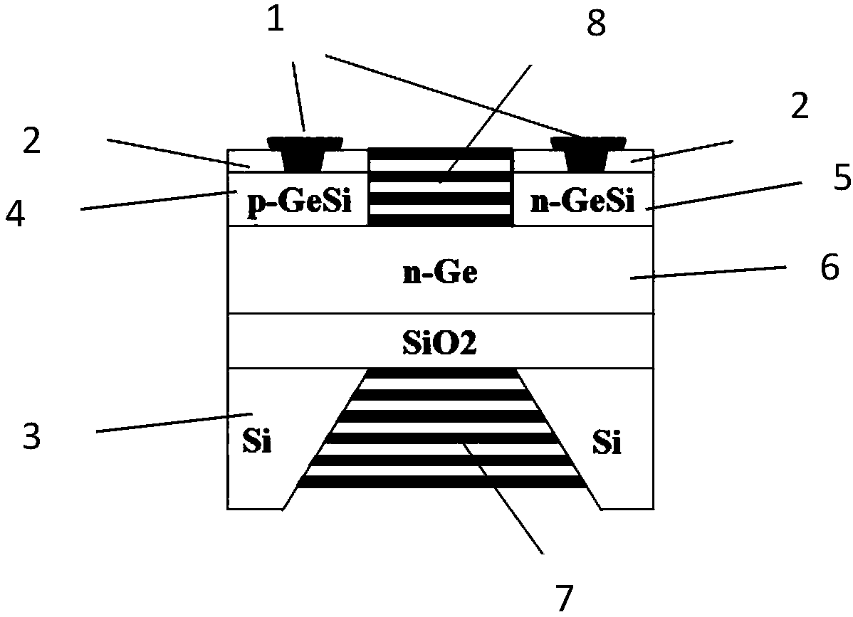
[0027] The purpose of the present invention is to carry out lateral heterostructure design on Ge light-emitting devices, supplemented by microcavity structure design, and realize p-GeSi / n-Ge / n by means of distributed Bragg reflector (DBR) structures at the top and bottom of the active layer -GeSi lateral structure high-efficiency light-emitting device, providing a method for preparing a lateral p-n-n microcavity structure Ge light-emitting device with simple process, compatible with mature silicon CMOS process and superior performance.

[0028] Such as figure 1 As shown, a Ge light-emitting device with a lateral p-n-n microcavity structure includes an active layer n-Ge layer 6, and the lower surface of the n-Ge layer 6 is Si / SiO 2 Structure 3, n-Ge layer 6 with Si / SiO 2 Structure 3 constitutes a highly dope...


PUM


Abstract

The invention discloses a transverse p-n-n microcavity-structured Ge light-emitting device. The light-emitting device comprises an active layer n-Ge layer; a Si / SiO<2> structure is on the lower surface of the n-Ge layer; the n-Ge layer and the Si / SiO<2> structure form a highly-doped n type GOI substrate; a bottom distributed Bragg reflection mirror is arranged at the bottom; a p-GeSi region and ann-GeSi region are arranged on the two sides of the upper surface of the n-Ge layer, and an active region is in the middle; the n-Ge layer is exposed at the bottom of the active region; a top distributed Bragg reflection mirror is arranged in the active region; electrodes of low-resistance conductive materials are arranged on the p-GeSi region and the n-GeSi region; and a silicon oxide passivationlayer is arranged on the surface of the light emitting device. A GeSi layer with high germanium component is arranged on the highly-doped n type GOI substrate in an epitaxial manner, and the Ge lightemitting device with the transverse p-n-n structure is realized, wherein the Ge component is 0.85, and an effective potential layer can be formed between GeSi and Ge, so that an effective limiting effect on electrons and holes can be played, so that Ge band light emitting efficiency can be further reinforced directly; and the method has the advantages of simple preparation process, compatibilitywith a mature silicon CMOS process, high operability, excellent light emitting performance and the like, and has extremely high application value.

Description

technical field [0001] The invention relates to the field of semiconductors, in particular to a Ge light-emitting device with a lateral p-n-n microcavity structure and a preparation method thereof. Background technique [0002] Silicon-based light-emitting devices are one of the important components to realize silicon-based optoelectronic integrated circuits. At present, there are two main methods for preparing silicon-based light-emitting devices, one is the preparation of Si-based III-V hybrid integrated lasers, and the other is the preparation of new Si-based group IV light-emitting devices. The main research directions for Si-based III-V hybrid integrated lasers can be summarized into three types: First, the mature III-V semiconductor laser devices are packaged on Si-based chips by flip-chip welding technology. Although this method can ensure that the laser has Good performance, but the technical level is high, and the current technical level is not enough for mass prod...

Claims


Application Information

Patent Timeline
Patent Type & Authority Applications(China)
IPC IPC(8): H01L33/34H01L33/10H01L33/44H01L33/02
CPCH01L33/02H01L33/10H01L33/34H01L33/44
Inventor 黄诗浩郑启强曹世阳谢文明李天建汪涵聪陈彩云黄靖
Owner FUJIAN UNIV OF TECH
Why Eureka
Try Eureka