Semiconductor package structure with pin sidewall tin climbing function and its manufacturing process

A technology of packaging structure and manufacturing process, applied in semiconductor/solid-state device manufacturing, semiconductor devices, semiconductor/solid-state device components, etc., can solve problems such as delamination, and achieve the effect of saving equipment costs

Active Publication Date: 2020-03-06
JCET GROUP CO LTD
View PDF12 Cites 0 Cited by
  • Summary
  • Abstract
  • Description
  • Claims
  • Application Information

AI Technical Summary

Problems solved by technology

[0009] However, this kind of packaging structure that forms L-shaped outer leads or C-shaped outer leads by cutting ribs also has the following defects when forming L-shaped outer leads or C-shaped outer leads: first, when performing outer When the pins are formed, the outer pins are bent toward the side of the plastic package, Figure 1G and Figure 1H The inner pin at A will be affected by the rebound force of the metal, which will cause the metal pin to have the stress of being pulled away from the plastic package downwards, and in the case of this downward force, it is easy to cause A. Delamination occurs between the upper surface of the inner pin and the lower surface of the molding compound

Method used


Image

  • Semiconductor package structure with pin sidewall tin climbing function and its manufacturing process
  • Semiconductor package structure with pin sidewall tin climbing function and its manufacturing process
  • Semiconductor package structure with pin sidewall tin climbing function and its manufacturing process

Examples


Embodiment 1

[0074] Example 1: Two electroplating forms a thickened base island

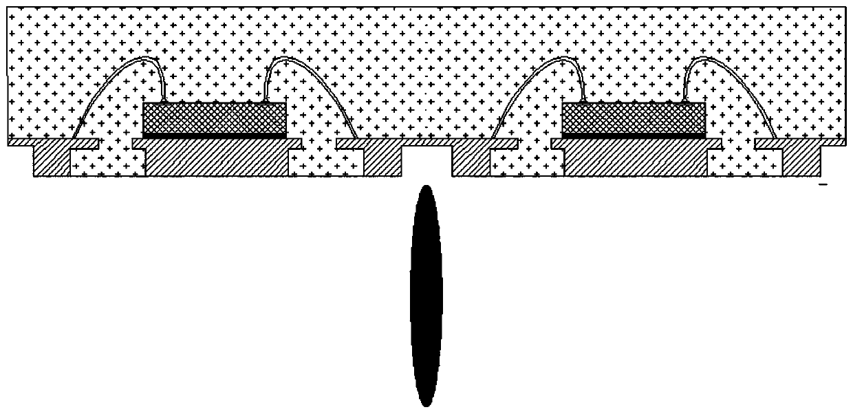
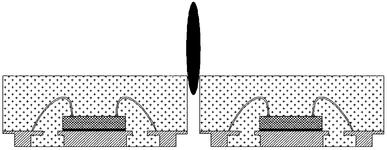
[0075] like figure 2 , image 3 As shown, in this embodiment, a semiconductor package structure with the function of tin-climbing pin sidewalls includes a base island 1 and a pin 2, and the pin 2 and the base island 3 are metal circuit layers formed by electroplating. The pins 2 are arranged around the base island 3, the front of the base island 1 is provided with a thickened layer 3, the base island 1 and the thickened layer 3 form a thickened base island, and the height of the thickened base island is high Based on the height of the pin 2, the pin 2 includes a plane part 2.1 and a side wall part 2.3, the side wall part 2.3 is located outside the plane part 2.1, and an arc part is passed between the plane part 2.1 and the side wall part 2.3 2.2 Smooth transition connection, the convex surface of the arc-shaped part 2.2 faces the outer lower side, the front of the thickened base island is provided with a c...

Embodiment 2

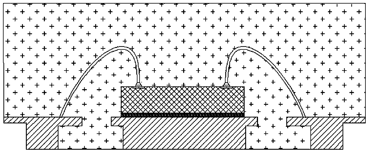
[0087] Embodiment 2: Copper sheet is arranged under the chip

[0088] Such as Figure 16 , Figure 17 As shown, in this embodiment, a semiconductor package structure with the function of tin-climbing pin sidewalls includes a copper sheet 8, a pin 2, and a base island 1. The surface of the copper sheet 8 is provided with a base island 1, so The pin 2 and the base island 1 are metal circuit layers formed by electroplating, the pin 2 is arranged around the copper sheet 8, the pin 2 includes a plane part 2.1 and a side wall part 2.3, and the side wall part 2.3 is located at On the outside of the plane part 2.1, the plane part 2.1 and the side wall part 2.3 are smoothly transitioned through the arc part 2.2, the convex surface of the arc part 2.2 faces the outer lower side, and the front of the base island 1 is connected by an adhesive substance or The solder 4 is provided with a chip 5, and the chip 5 is electrically connected to the pin 2 through the metal bonding wire 6. The p...


PUM


Abstract

The present invention relates to a semiconductor packaging structure with the function of tin-climbing pin sidewalls and its manufacturing process. The structure includes a base island and pins. The pins include a plane part and a sidewall part. On the outside of the planar part, the planar part and the side wall part are connected by a smooth transition through an arc part, the convex surface of the arc part faces the outer lower side, and a chip is arranged on the front of the base island, and the chip is connected by a metal bonding wire To form electrical connection with the pins, the base island, the pins and the peripheral area of ​​the chip are encapsulated with a molding compound, and the outer surfaces of the plane part, the arc part and the side wall part are exposed to the molding compound. When the present invention is soldering the PCB, the solder can climb to a higher height along the vertical side wall, thereby increasing the bonding area between the solder and the pins, and at the same time, the air at the pins can be discharged along the convex arc, thereby improving the reliability of the product. Welding performance, welding reliability and visual inspection of welding status.

Description

technical field [0001] The invention relates to a semiconductor packaging structure with the function of tin climbing on the side wall of a pin and a manufacturing process thereof, belonging to the technical field of semiconductor packaging. Background technique [0002] With the development of modern technology, semiconductor packaging has been widely used. Its extensive applications in radar, remote control telemetry, aerospace, etc. put forward higher and higher requirements for its reliability. The failure caused by poor soldering of semiconductors has attracted more and more attention, because this failure is often fatal and irreversible. Therefore, it is very important to get a good soldering reliability in the semiconductor industry. The tin layer on the soldering surface of the semiconductor can make the soldering stronger, especially for automotive electronics. [0003] As we all know, QFN (Quad Flat No-lead Package, four-sided leadless flat package) and DFN (Duad...

Claims


Application Information

Patent Timeline
Patent Type & Authority Patents(China)
IPC IPC(8): H01L23/31H01L23/48H01L23/488H01L21/56
CPCH01L21/56H01L23/31H01L23/481H01L23/488H01L21/60H01L2224/48091H01L2224/48247H01L2224/97H01L2924/181H01L2924/00014H01L2924/00012
Inventor 王亚琴梁志忠刘恺
Owner JCET GROUP CO LTD
Why Eureka
Try Eureka