Copper-clad plate, printed circuit plate and manufacturing method thereof

A technology of printed circuit boards and copper clad laminates, which is applied in the fields of printed circuit manufacturing, printed circuits, printed circuit components, etc., and can solve problems such as copper layer blistering, poor metal bonding, and poor reliability

Active Publication Date: 2012-09-19
SHENZHEN WUZHU TECH +2
View PDF5 Cites 10 Cited by
  • Summary
  • Abstract
  • Description
  • Claims
  • Application Information

AI Technical Summary

Problems solved by technology

However, due to its own characteristics, ceramics have poor bonding force with copper or other metals on the surface, and copper layer blisters and warping often occur, resulting in insufficient product yield and poor reliability.

Method used


Image

  • Copper-clad plate, printed circuit plate and manufacturing method thereof
  • Copper-clad plate, printed circuit plate and manufacturing method thereof
  • Copper-clad plate, printed circuit plate and manufacturing method thereof

Examples


Embodiment Construction

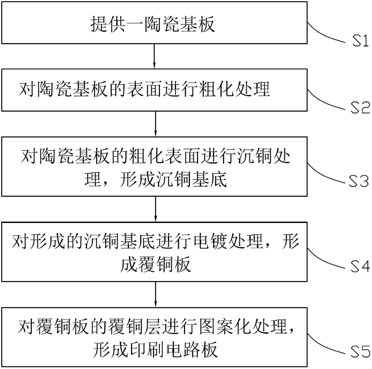
[0024] Specific embodiments of the present invention will be described in detail below in conjunction with the accompanying drawings.

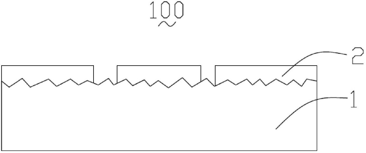
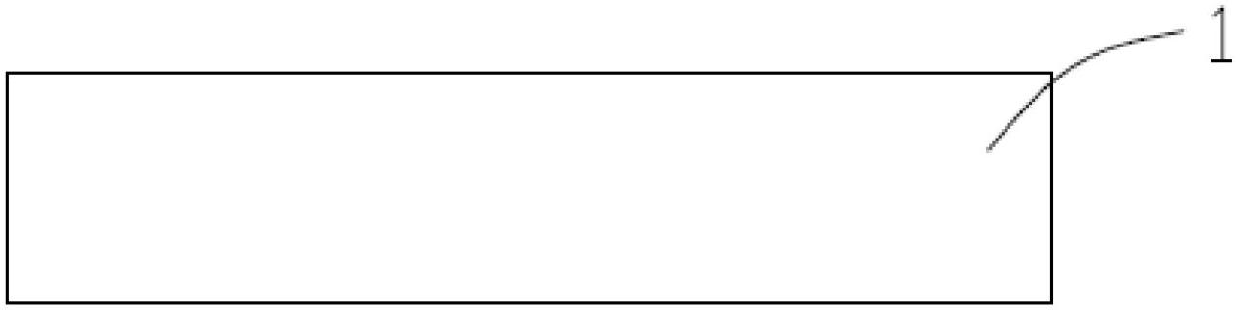
[0025] see figure 1 , figure 1 It is a schematic cross-sectional structure diagram of a printed circuit board (Printed Circuit Board, PCB) of the present invention. The printed circuit board 100 includes a ceramic substrate 1 and a patterned copper layer 2 disposed on the ceramic substrate 1 .

[0026] Specifically, the surface of the ceramic substrate 1 is roughened to form a roughness of 50 microns to 150 microns, which is conducive to the tight bonding of the patterned copper layer 2 and prevents the metal layer from falling off and warping.

[0027] The patterned copper layer 2 can also be replaced by a common conductive material such as an aluminum layer, a silver layer, or a gold layer according to actual needs, which is not specifically limited here. The patterned copper layer 2 in this embodiment may be formed on the ceramic substra...


PUM

PropertyMeasurementUnit
surface roughnessaaaaaaaaaa
thicknessaaaaaaaaaa
surface roughnessaaaaaaaaaa

Abstract

The invention relates to a manufacturing method of a copper-clad plate. The method comprises the following steps of: providing a ceramic baseplate, carrying out roughening treatment on the surface of the ceramic baseplate; carrying out copper deposition treatment on the ceramic surface after roughening to form a copper-deposited base; and carrying out electroplating treatment on the formed copper-deposited base to form the copper-clad plate. The invention also provides a manufacturing method of a printed circuit plate based on the manufacturing method of the copper-clad plate. The invention further provides the copper-clad plate and the printed circuit plate. The printed circuit plate has the advantages of good electrical property, good mechanical property and high reliability.

Description

technical field [0001] The invention relates to a copper-clad laminate, a printed circuit board and a manufacturing method thereof, in particular to a copper-clad laminate with ceramics as a substrate, a printed circuit board and a manufacturing method thereof. Background technique [0002] Printed Circuit Board (PCB) is the basis of almost any electronic product and appears in almost every electronic device. Generally speaking, if there are electronic components in a certain device, they are also integrated on printed circuit boards of various sizes. [0003] As the functions of electronic products are enhanced day by day, their popularity is getting higher and higher. The requirements for printed circuit boards used in electronic products have also increased accordingly. [0004] Common printed circuit boards generally use FR-4 (epoxy resin) as the copper clad laminate of the substrate. However, the printed circuit board made of FR-4 material has a large dielectric loss...

Claims


Application Information

Patent Timeline
Patent Type & Authority Applications(China)
IPC IPC(8): B32B15/20B32B18/00B32B37/00H05K1/02H05K3/02
Inventor 曾令雨徐学军李春明林文乾
Owner SHENZHEN WUZHU TECH
Why Eureka
Try Eureka