Silicon-based laser device

A laser and silicon-based technology, applied in the field of optical communications, can solve problems such as low luminous efficiency and restrictions on breakthroughs in silicon photonics technology

Active Publication Date: 2018-06-01
HISENSE BROADBAND MULTIMEDIA TECH
View PDF15 Cites 5 Cited by
  • Summary
  • Abstract
  • Description
  • Claims
  • Application Information

AI Technical Summary

Problems solved by technology

However, since silicon is an indirect bandgap material, its luminous efficiency is extremely low, and it is not suitable as a light-emitting device, which seriously restricts the further breakthrough of silicon photonics technology in the field of optical communication.

Method used


Image

  • Silicon-based laser device
  • Silicon-based laser device
  • Silicon-based laser device

Examples


Embodiment Construction

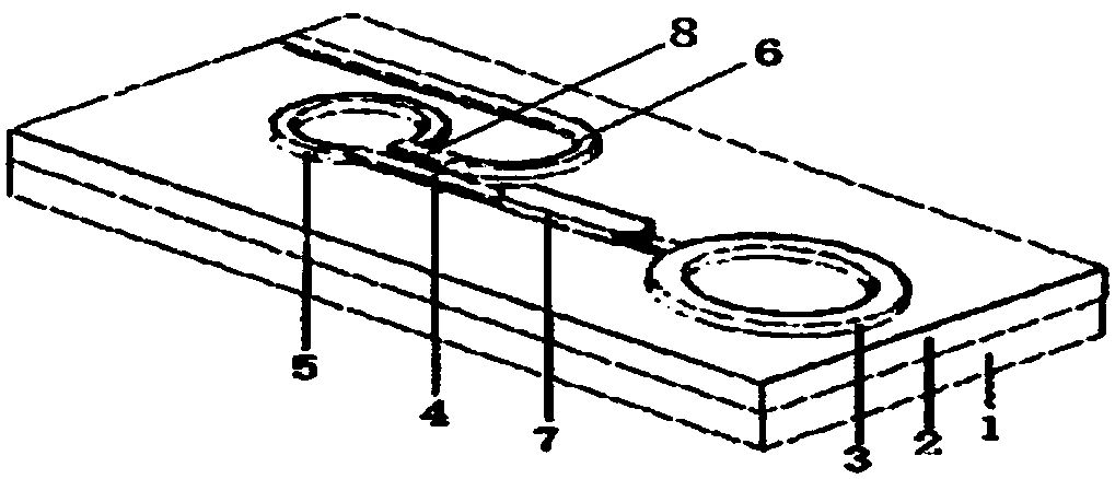
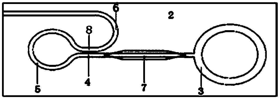
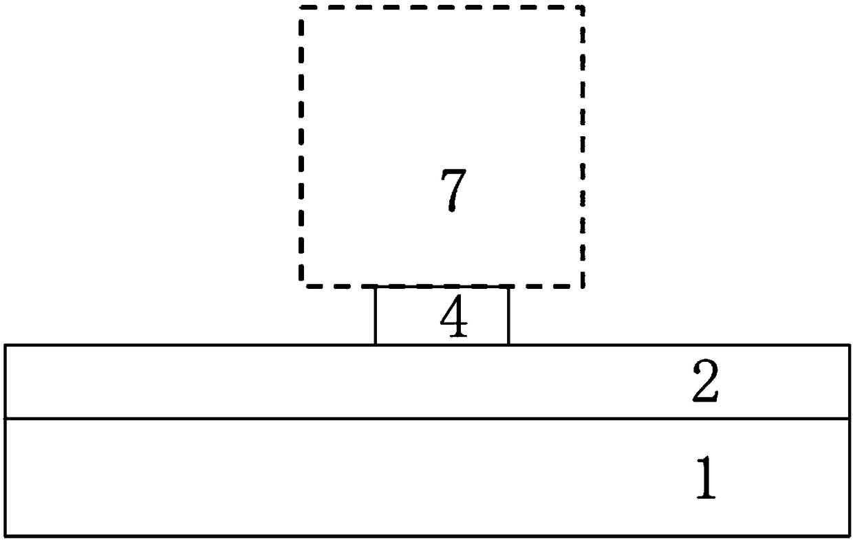
[0021] As mentioned in the background technology, in order to solve the technical problem that silicon has low luminous efficiency and is not suitable as a light-emitting device, people try to bond the semiconductor light-emitting chip on the silicon photonic chip through bonding technology, and use the semiconductor light-emitting chip as a silicon photonic chip The light-injecting method is provided to fabricate a light-emitting device.

[0022] Based on this, the inventors of the present application hope to propose a silicon-based optical device to solve the above technical problems.

[0023] The present application will be described in further detail below in conjunction with the accompanying drawings, but it is not intended to limit the present application. Hereinafter, for the convenience of description, the "left", "right", "upper" and "lower" referred to hereinafter are consistent with the directions of left, right, upper and lower in the accompanying drawings, and "fi...


PUM


Abstract

The invention proposes a silicon-based laser device, which relates to the technical field of optical communication. The silicon-based laser device comprises a silicon substrate and a semiconductor light emitting chip, wherein an annular closed silicon waveguide, a connection silicon waveguide, an annular open silicon waveguide and an output silicon waveguide are formed on the surface of the silicon substrate; light emitted from the semiconductor light emitting chip enters the annular closed silicon waveguide and the annular open silicon waveguide via the connection silicon waveguide for resonance; light reflection occurs at a junction of the annular open silicon waveguide and the output silicon waveguide, so that part of the light is reflected back to the connection silicon waveguide for resonance, and the other part of the light is reflected toward the output silicon waveguide to be output externally. The silicon-based laser device provided by the invention can be used for resonatingand reflecting the light provided by the semiconductor light emitting chip so as to finally realize laser output, thereby improving the silicon light emitting efficiency.

Description

technical field [0001] The present application relates to the technical field of optical communication, in particular to a silicon-based laser. Background technique [0002] With the increasingly higher bandwidth requirements for information transmission, traditional optical modules based on III-V InP-based DFB (Distributed Feedback Laser, distributed feedback laser) lasers are difficult to achieve modulation higher than 25G due to their own material limitations The bandwidth cannot meet people's needs. Therefore, people hope that the silicon photonics platform can achieve technological breakthroughs in the field of optical module data transmission. [0003] At present, silicon optical devices such as high-speed silicon optical modulators, high-speed detectors, low-loss transmission waveguides, and wavelength division multiplexing have been fabricated on silicon optical platforms, and the mutual integration of various functional devices has been realized. Single-channel in...

Claims


Application Information

Patent Timeline
Patent Type & Authority Applications(China)
IPC IPC(8): H01S5/02H01S5/10
CPCH01S5/021H01S5/10
Inventor 隋少帅
Owner HISENSE BROADBAND MULTIMEDIA TECH
Why Eureka
Try Eureka