High-power pulse width tunable semiconductor laser module

A semiconductor, high-power technology, applied in the field of high-power pulse width tunable semiconductor laser modules, can solve the problems of narrow pulse width tunable range, low photoelectric conversion efficiency, high cost, etc., and achieve fast rising edge of optical pulse and easy processing system The effect of integrated, high power output

Inactive Publication Date: 2019-07-05
杭州晟创激光科技有限公司
View PDF0 Cites 5 Cited by
  • Summary
  • Abstract
  • Description
  • Claims
  • Application Information

AI Technical Summary

Problems solved by technology

[0002] Laser processing is more and more widely used. Existing laser processing light sources are mainly solid-state lasers and fiber lasers, which have the disadvantages of large volume, high cost, low photoelectric conversion efficiency, and narrow pulse width tunable range. The patent of the present invention can be very good to solve the above problems

Method used


Image

  • High-power pulse width tunable semiconductor laser module
  • High-power pulse width tunable semiconductor laser module
  • High-power pulse width tunable semiconductor laser module

Examples


Embodiment 1

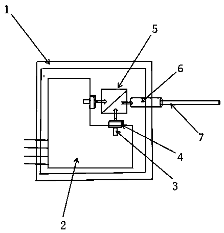
[0023] like figure 1 As shown, the laser module consists of an oxygen-free copper heat dissipation shell (1), a ceramic drive circuit substrate (2), a polarization beam combining prism (5), a self-focusing lens (6) and a coupling output optical fiber (7).

[0024] A 915nm (or 940nm / 976nm / 980nm) high-power semiconductor laser chip (3) is packaged on an aluminum nitride ceramic substrate (2) with a driving circuit.

[0025] Further, the ceramic driving circuit substrate (2) is welded to the base of the oxygen-free copper casing (1) through indium solder, silver glue or other solders.

[0026] Further, the fast-axis collimating mirror (4) is fixed on the front end of the ceramic substrate according to the working distance of the lens through ultraviolet glue, so as to collimate and compress the fast axis of the laser.

[0027] Further, the two beams of light enter the self-focusing lens (6) through the polarization beam combining prism (5), and are coupled into the optical fiber...

Embodiment 2

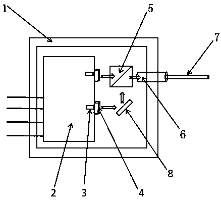
[0029] like figure 2 As shown, the laser module consists of an oxygen-free copper heat dissipation shell (1), a ceramic drive circuit substrate (2), a polarization beam combining prism (5), a self-focusing lens (6), a coupling output fiber (7), and a mirror (8) composition.

[0030] A 915nm (or 940nm / 976nm / 980nm) high-power semiconductor laser chip (3) is packaged on an aluminum nitride ceramic substrate (2) with a driving circuit.

[0031] Further, the ceramic driving circuit substrate (2) is welded to the base of the oxygen-free copper casing (1) through indium solder, silver glue or other solders.

[0032] Further, the fast-axis collimating mirror (4) is fixed on the front end of the ceramic substrate according to the working distance of the lens through ultraviolet glue, so as to collimate and compress the fast axis of the laser.

[0033] Further, after the light emitted by the laser chip 31 is reflected by the mirror (8), it enters the self-focus lens (6) with the ligh...


PUM


Abstract

The invention discloses a high-power pulse width tunable semiconductor laser light source module, which utilizes optoelectronic integrated packaging technology to integrate laser drive control and a laser for package, performs fiber output on semiconductor laser coupling through a polarization combining technique and a self-focusing lens fiber coupling technology to achieve high peak power, smallvolume and narrow pulse, and uses an external trigger signal to realize pulse width tunable function. Compared with fiber lasers and solid lasers, the high-power pulse width tunable semiconductor laser light source module has obvious advantages in performance, cost and photoelectric conversion efficiency.

Description

technical field [0001] The invention relates to a high-power pulse width tunable semiconductor laser module, which belongs to the field of high-power lasers. Background technique [0002] Laser processing is more and more widely used. Existing laser processing light sources are mainly solid-state lasers and fiber lasers, which have the disadvantages of large volume, high cost, low photoelectric conversion efficiency, and narrow pulse width tunable range. The patent of the present invention can be very good to solve the above problems. Contents of the invention [0003] The purpose of the present invention is to propose a high-power adjustable pulse width semiconductor laser module, which realizes a nanosecond-level narrow pulse, high peak power, and compact light source module by integrating photoelectric packaging, polarization beam combining technology, and self-focusing lens fiber coupling technology structure. [0004] The technical solution adopted by the present in...

Claims


Application Information

Patent Timeline
Patent Type & Authority Applications(China)
IPC IPC(8): H01S5/024H01S5/022H01S5/042G02B6/42
CPCG02B6/4201G02B6/4204G02B6/428H01S5/02469H01S5/042H01S5/02251
Inventor 董武
Owner 杭州晟创激光科技有限公司
Why Eureka
Try Eureka