Equipment and method for reducing defects of wafer holes

A wafer and cavity technology, used in electrolytic components, electrolytic processes, circuits, etc., can solve problems such as reducing the ability of electrochemical polishing to fill holes, reducing the contact effect of conductive seed layers, and voiding.

Inactive Publication Date: 2018-06-05
HUAIAN IMAGING DEVICE MFGR CORP
View PDF9 Cites 4 Cited by
  • Summary
  • Abstract
  • Description
  • Claims
  • Application Information

AI Technical Summary

Problems solved by technology

Since the various grooves and through holes on the front of the wafer are facing downward, the gas in the grooves and through holes cannot be discharged in time when the wafer enters the electrolytic solution, thus making the electrolytic solution and the wafer conductive The contact effect of the seed layer is reduced, which reduces the hole filling ability during the electrochemical polishing (ECP) process, which eventually leads to void defects

Method used


Image

  • Equipment and method for reducing defects of wafer holes
  • Equipment and method for reducing defects of wafer holes
  • Equipment and method for reducing defects of wafer holes

Examples


Embodiment Construction

[0040] Various exemplary embodiments of the present disclosure will now be described in detail with reference to the accompanying drawings. It should be noted that relative arrangements of components and steps, numerical expressions and numerical values ​​set forth in these embodiments do not limit the scope of the present disclosure unless specifically stated otherwise.

[0041] The following description of at least one exemplary embodiment is merely illustrative in nature and in no way intended as any limitation of the disclosure, its application or uses.

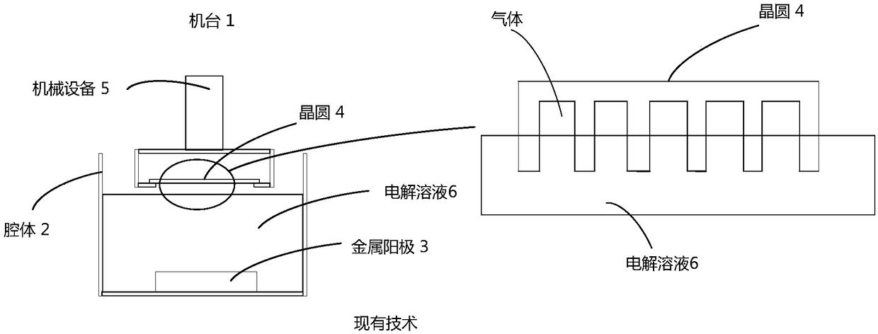
[0042] figure 1 A schematic diagram of a machine 1 for electroplating wafers in the prior art is shown. The electroplating machine 1 generally includes a cavity 2 filled with an electrolytic solution 6 and the cavity 2 includes a metal anode 3 immersed in the bottom of the electrolytic solution, the metal anode 3 and the liquid surface of the electrolytic solution 6 are generally substantially parallel. The electrolytic...


PUM

PropertyMeasurementUnit
angleaaaaaaaaaa

Abstract

The application relates to a machine board for electroplating a wafer. The machine board comprises a cavity, wherein an opening is formed in the surface of the cavity and used for receiving the waferso as to feed the wafer into the cavity; a metal anode is arranged in the cavity and can be filled with an electrolytic solution; the metal anode is basically perpendicular to the liquid level of theelectrolytic solution.

Description

technical field [0001] The present invention relates to a device and method for electroplating wafers, and more particularly relates to a device and method capable of reducing wafer void defects in the process of electroplating wafers. Background technique [0002] Fabrication of semiconductor devices generally requires the formation of conductive layers on semiconductor wafers. For example, conductive leads on the wafer are typically formed by electroplating (depositing) a conductive layer such as copper on the wafer and within the patterned trenches / vias. Specifically, a conductive seed layer is first deposited in the trenches and on the surface of the semiconductor substrate, for example by physical vapor deposition. An electroplating process is then used to form a conductive layer on the conductive seed layer. [0003] The electrolytic solution is in electrical contact with the surface of the wafer to be plated (the surface to be plated of the wafer is hereinafter refe...

Claims


Application Information

Patent Timeline
Patent Type & Authority Applications(China)
IPC IPC(8): C25D7/12C25D17/00
Inventor 吴明吴孝哲林宗贤吴龙江薛超马亚辉
Owner HUAIAN IMAGING DEVICE MFGR CORP
Why Eureka
Try Eureka