AMOLED pixel repairing method

A pixel, thin film transistor technology, applied in the field of OLED display, can solve the problems of high laser energy, long repair time, large area occupied, etc., to achieve the effect of reducing laser energy and saving repair time

Inactive Publication Date: 2018-06-05
WUHAN CHINA STAR OPTOELECTRONICS SEMICON DISPLAY TECH CO LTD
View PDF8 Cites 6 Cited by
  • Summary
  • Abstract
  • Description
  • Claims
  • Application Information

AI Technical Summary

Problems solved by technology

[0009] AMOLED display devices will be inspected after the manufacturing process is completed. If AMOLED pixels with abnormal display are detected, they need to be repaired. The common repair method is to use laser to break down the organic light-emitting diode D, so that the pixels with abnormal display will be darkened. However, due to The organic light-emitting diode D occupies a large area in the pixel area, the laser energy used to completely break down the organic light-emitting diode D is relatively large, and the repair time is also relatively long

Method used


Image

  • AMOLED pixel repairing method
  • AMOLED pixel repairing method
  • AMOLED pixel repairing method

Examples


Embodiment Construction

[0043] In order to further illustrate the technical means adopted by the present invention and its effects, the following describes in detail the preferred embodiments of the present invention and the accompanying drawings.

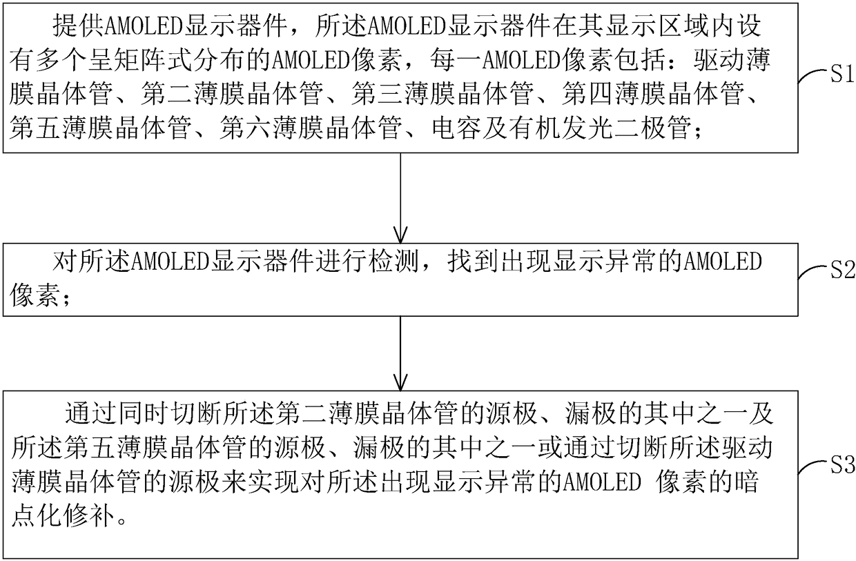
[0044] See image 3 , The present invention provides an AMOLED pixel repair method, including the following steps:

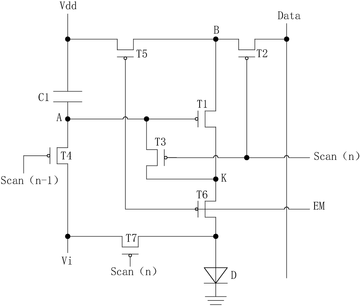
[0045] Step S1: Provide an AMOLED display device, the AMOLED display device is provided with a plurality of AMOLED pixels distributed in a matrix in its display area. Each AMOLED pixel has a 7T1C or 6T1C structure with compensation function.

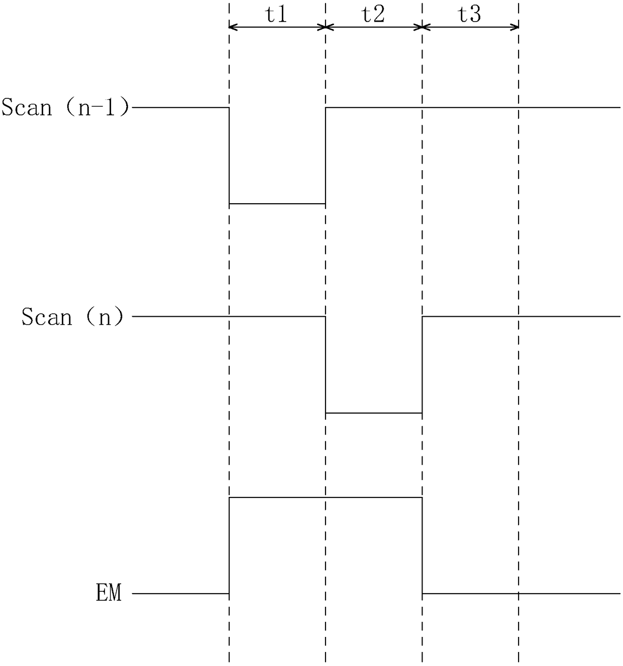
[0046] Please refer to figure 1 Taking the 7T1C structure as an example, each AMOLED pixel includes: driving thin film transistor T1, second thin film transistor T2, third thin film transistor T3, fourth thin film transistor T4, fifth thin film transistor T5, sixth thin film transistor T6, The seventh thin film transistor T7, the capacitor C1 and the organic light emitting diode D.

[0047] Specifically: the...


PUM


Abstract

The invention provides an AMOLED pixel repairing method. According to the invention, a path for transmitting a data signal (Data) to a driving thin film transistor (T1) in an AMOLED pixel which is abnormal in display is cut off and a path for transmitting power voltage (Vdd) to the driving thin film transistor (T1) in the AMOLED pixel which is abnormal in display is cut off through simultaneouslycutting off one of a source electrode and a drain electrode of a second thin film transistor (T2) and one of a source electrode and a drain electrode of a fifth thin film transistor (T5) or through cutting off a source electrode of the driving thin film transistor (T1), thereby realizing dark spot repairing for the AMOLED pixel which is abnormal in display, being capable of reducing laser energy required by the repairing, and saving the repairing time.

Description

Technical field [0001] The present invention relates to the field of OLED display technology, in particular to a method for repairing AMOLED pixels. Background technique [0002] Flat display devices have many advantages such as thin body, power saving, and no radiation, and have been widely used. Existing flat display devices mainly include liquid crystal display devices (Liquid Crystal Display, LCD) and organic light emitting diode display devices (Organic Light Emitting Display, OLED). [0003] OLED display devices have excellent characteristics such as self-luminous, no backlight, high contrast, thin thickness, wide viewing angle, fast response speed, can be used for flexible panels, wide operating temperature range, simple structure and manufacturing process, etc., are considered It is the emerging application technology of the next generation flat panel display. [0004] OLED display devices can be divided into passive OLED (PMOLED) and active OLED (AMOLED) according to the d...

Claims


Application Information

Patent Timeline
Patent Type & Authority Applications(China)
IPC IPC(8): G09G3/00H01L27/32
CPCG09G3/006H10K59/121
Inventor 陈彩琴王一伊王少波
Owner WUHAN CHINA STAR OPTOELECTRONICS SEMICON DISPLAY TECH CO LTD
Why Eureka
Try Eureka