Semiconductor structures and methods of forming them

A semiconductor and transistor area technology, applied in the field of semiconductor structure and its formation, can solve the problems of poor overall performance of semiconductor devices, and achieve the effects of avoiding adverse effects, improving overall performance, and optimizing electrical performance.

Active Publication Date: 2019-11-01
SEMICON MFG INT (SHANGHAI) CORP +1
View PDF3 Cites 0 Cited by
  • Summary
  • Abstract
  • Description
  • Claims
  • Application Information

AI Technical Summary

Problems solved by technology

[0004] However, the performance of the SRAM in the semiconductor device formed in the prior art needs to be further improved, so that the overall performance of the semiconductor device is poor

Method used


Image

  • Semiconductor structures and methods of forming them
  • Semiconductor structures and methods of forming them
  • Semiconductor structures and methods of forming them

Examples


Embodiment Construction

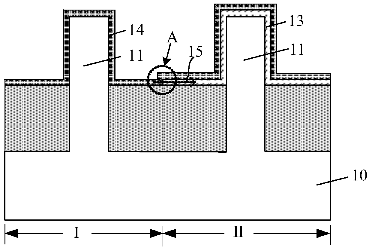
[0014] It can be seen from the background art that the performance of Static Random Access Memory (SRAM, Static Random Access Memory) in semiconductor devices needs to be improved. refer to figure 1 , shows a schematic diagram of a cross-sectional structure corresponding to a method for forming a semiconductor structure, and analyzes the reason why the performance of the SRAM needs to be improved in combination with the method for forming a semiconductor structure.

[0015] The forming method includes: providing a base, the base includes a substrate 10 and discrete fins 11 located on the substrate 10, the substrate 10 includes a pull-down transistor region I for forming a pull-down transistor and a fin for forming a pull-down transistor. The pull-up transistor region II of the pull-up transistor, and the pull-down transistor region I and the pull-up transistor region II are adjacent regions; form a P-type work spanning the pull-down transistor region I and the pull-up transist...


PUM


Abstract

A semiconductor structure and its forming method, comprising: providing a substrate, including an N-type logic region, a P-type logic region, and adjacent pull-up transistor regions and pull-down transistor regions; forming a first work function layer on a gate dielectric layer; removing the first work function layer of the N-type logic region and the pull-down transistor region; forming a second work function layer on the remaining first work function layer and the gate dielectric layer; removing the second work function layer of the second N-type threshold voltage region; An N-type work function layer is formed on the remaining second work function layer and the second N-type threshold voltage region. Compared with the scheme of only forming an N-type work function layer in the pull-down transistor region, the second work function layer of the present invention covers the sidewall of the first work function layer at the junction of the pull-up transistor region and the pull-down transistor region, and also covers the second work function layer of the pull-up transistor region. On the top of the first work function layer, the diffusion path of metal ions in the N-type work function layer to the first work function layer in the pull-up transistor region is increased to optimize the electrical performance of the SRAM.

Description

technical field [0001] The invention relates to the field of semiconductors, in particular to a semiconductor structure and a forming method thereof. Background technique [0002] In the current semiconductor industry, integrated circuit products can be mainly divided into three types: logic, memory and analog circuits, among which memory devices account for a considerable proportion of integrated circuit products. With the development of semiconductor technology, storage devices are more widely used, and the storage device and other device regions need to be formed on a chip at the same time to form an embedded semiconductor storage device. For example, to embed the storage device in the central processing unit, it is necessary to make the storage device compatible with the embedded central processing unit platform, and maintain the specifications and corresponding electrical performance of the original storage device. [0003] Generally, the memory device needs to be comp...

Claims


Application Information

Patent Timeline
Patent Type & Authority Patents(China)
IPC IPC(8): H01L21/8244H01L27/11
CPCH10B10/12H01L21/823842H01L29/4966H01L29/517H01L29/66545H01L21/28185H01L21/82345H01L27/092H01L21/823821H01L27/0924H10B10/18H01L29/42372H01L21/82385H01L29/4958H01L21/28079H01L29/785H01L27/0922H01L21/28088
Inventor 李勇
Owner SEMICON MFG INT (SHANGHAI) CORP
Why Eureka
Try Eureka