A field effect tube

A field effect tube and field effect technology, which is applied in the direction of semiconductor/solid-state device parts, semiconductor devices, electrical components, etc., can solve the problem of inability to resist radiation, and achieve the effect of reducing irradiation dose, reducing impact and improving reliability.

Active Publication Date: 2020-12-04
GUIZHOU MINZU UNIV
View PDF4 Cites 0 Cited by
  • Summary
  • Abstract
  • Description
  • Claims
  • Application Information

AI Technical Summary

Problems solved by technology

[0004] In view of the above problems, the present invention provides a field effect tube, which effectively solves the technical problem that the existing field effect tube cannot resist radiation

Method used


Image

  • A field effect tube
  • A field effect tube
  • A field effect tube

Examples


Embodiment Construction

[0026] In order to more clearly illustrate the embodiments of the present invention or the technical solutions in the prior art, the specific implementation manners of the present invention will be described below with reference to the accompanying drawings. Obviously, the accompanying drawings in the following description are only some embodiments of the present invention, and those skilled in the art can obtain other accompanying drawings based on these drawings and obtain other implementations.

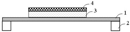
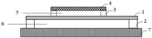
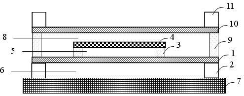
[0027] Such as figure 1 Shown is a schematic structural diagram of an embodiment of a field effect transistor provided by the present invention. It can be seen from the figure that the field effect transistor includes: a first channel layer 1, a first insulating layer 3, and a gate 4 And the first electrode 2 , wherein the first electrode 2 is located on one side surface of the first channel layer 1 , the first insulating layer 3 is located on the other surface of the first channe...


PUM


Abstract

The invention provides a field-effect transistor. The field-effect transistor comprises a first channel layer, a first insulation layer, a grid and a first electrode, wherein the first electrode is arranged on a surface of one side of the first channel layer, the first insulation layer is arranged on the other surface of the first channel layer, the grid is arranged on a surface of the first insulation layer, and the first channel layer and the grid are made of two-dimensional materials. Since the channel layer and the grid comprise the two-dimensional materials, the relatively high radiation-resistance capability of the field-effect transistor is greatly improved.

Description

technical field [0001] The invention relates to the technical field of semiconductors, in particular to a field effect transistor. Background technique [0002] With the rapid development of aerospace technology, various new and more intelligent spacecraft have emerged in space, and these intelligent spacecraft carry a large number of electronic devices. In addition, in future space exploration and space factories, a large number of robots will be required to replace human work, and powerful integrated electronic chips will also be required in these robots. However, spacecraft in space will be subject to various radiations, which will cause serious damage to integrated electronic chips, affect the performance of devices, and even damage these integrated electronic chips, causing irreparable losses. [0003] In addition, in the nuclear industry, a large number of intelligent chips are also required, especially in the rescue of nuclear accidents, it is necessary to use robots...

Claims


Application Information

Patent Timeline
Patent Type & Authority Patents(China)
IPC IPC(8): H01L29/06H01L29/10H01L29/16H01L29/24H01L29/78H01L23/552
CPCH01L23/552H01L29/0649H01L29/1033H01L29/1606H01L29/24H01L29/78
Inventor 刘江涛
Owner GUIZHOU MINZU UNIV
Why Eureka
Try Eureka