
Liquid crystal panel and manufacturing method thereof

A technology of liquid crystal panels and manufacturing methods, which is applied in the direction of instruments, nonlinear optics, optics, etc., can solve the problems of not meeting the precision requirements of the dispensing process, expensive dispensing equipment, and poor consistency, so as to improve the visual effect and viewing experience. Avoiding the circuit printing process and reducing production costs

Inactive Publication Date: 2018-06-22
HUIZHOU CHINA STAR OPTOELECTRONICS TECHNOLOGY CO LTD
View PDF6 Cites 14 Cited by
  • Summary
  • Abstract
  • Description
  • Claims
  • Application Information

AI Technical Summary

Problems solved by technology

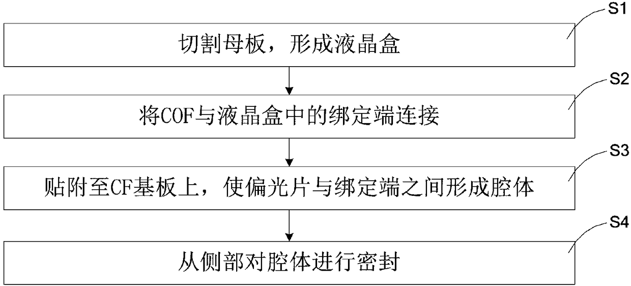
[0004] The first is to place the CF substrate outside as the viewing surface. At this time, the CF substrate is placed on the upper end of the TFT substrate, and a polarizer is installed on the CF substrate. Since the TFT substrate is connected to a COF (Chip On Film, overlay) after the CF substrate and polarizer are installed, crystal thin film), so the binding end connecting COF on it needs to exceed the CF substrate and the polarizer on it, and this leads to the need to process the binding end of the COF after the connection is completed, usually by dispensing Filling process, and if manual dispensing is used for dispensing filling, it is difficult to achieve standardized manufacturing due to random dispensing and poor consistency during manual work, and the fluctuation of dispensing effect is poor, which cannot meet the accuracy of dispensing process requirements, resulting in low yield and low production efficiency of LCD panels; if dispensing equipment is used for dispensing, the production cost of LCD panels is high due to the expensive dispensing equipment for this process;
[0005] The second is to place the TFT substrate externally as the viewing surface. At this time, after the COF is connected to the binding end of the TFT substrate, the metal traces on it will have an optical impact on the LCD panel. Therefore, it is necessary to print on the periphery of the TFT. Complicates the manufacturing process of the LCD panel and increases the production cost
[0006] The defects in the above existing two methods have all caused the borderless display to not be widely promoted and popularized.

Method used


Image

  • Liquid crystal panel and manufacturing method thereof
  • Liquid crystal panel and manufacturing method thereof
  • Liquid crystal panel and manufacturing method thereof

Examples


Embodiment 1

[0040] see figure 1 and figure 2 A liquid crystal panel provided in Embodiment 1 includes a TFT (Thin Film Transistor, thin film transistor) substrate 10 opposite to the backlight module, and a CF (Color filter, color filter) substrate disposed on the TFT substrate 10 20, and the liquid crystal 40 arranged between the TFT substrate 10 and the CF substrate 20, the liquid crystal 40 can be encapsulated between the TFT substrate 10 and the CF substrate 20 through the sealant 30, and the outer surfaces of the TFT substrate 10 and the CF substrate are respectively attached with The second polarizer 50 and the first polarizer 60 .

[0041] Wherein, each side of the CF substrate 20 covered on the sealant 30 is flush with each side of the sealant 30, it can be understood that the area where the liquid crystal 40 is provided forms the display area of ​​the liquid crystal panel; In the setting of the fixed end, at least one end surface of the TFT substrate 10 exceeds the end surface ...

Embodiment 2

[0056] When the binding end 10-1 on the TFT substrate 10 is wider, if the filling method in Embodiment 1 is selected, the cavity between the first polarizer 60 and the binding end 10-1 cannot be fully filled. Therefore, This embodiment is a further improvement on the filling method in Embodiment 1. The difference between this embodiment and Embodiment 1 is that the filling method of the encapsulant is different. For other structures, you can refer to the scheme in Embodiment 1. Let me repeat.

[0057] Specifically, see Figure 4 , Figure 5 and Figure 6 The filling method of the cavity of the liquid crystal panel in the second embodiment is as follows: firstly complete the melting and filling of the first encapsulant 701, that is, before attaching the first polarizer 60 on the CF substrate 20, the binding end 10- 1. Paste a thermoplastic adhesive film on top, and then hot press when attaching the first polarizer 60 to melt and solidify the thermoplastic adhesive film to fo...


PUM


Abstract

The invention discloses a liquid crystal panel. The panel comprises a TFT substrate, a CF substrate disposed on the TFT substrate, a liquid crystal filled between the TFT substrate and the CF substrate and a first polarizer attached to the outer surface of the CF substrate, at least one end surface of the TFT substrate extends beyond the side end surface of the CF substrate to form a binding end for connecting COF, the first polarizer completely covers the TFT substrate, the first polarizer, the binding end and the end surface of the binding end are provided with packaging adhesives, and the COF portion near the end surface of the binding end is wrapped in the packaging adhesives. The invention also discloses a manufacturing method of the liquid crystal panel. The liquid crystal panel firstly connects the binding end on the TFT substrate with the COF, and then attaches the polarizer, which does not need to fill the bare binding end through dispensing, reduces the production costs, avoids circuit printing processing caused by the externally arranged TFT substrate, and simplifies the process.

Description

technical field [0001] The invention relates to the technical field of liquid crystal display, and more specifically, it relates to a liquid crystal panel and a manufacturing method thereof. Background technique [0002] The bezel-less (Bezel Less) machine of the liquid crystal display has gradually become a popular design trend. A bezel-less display refers to a display device with an extremely narrow screen frame. Design, one of its advantages is its outstanding appearance. Compared with the monitors with thick borders in the past, borderless can bring a truly horizontal screen, so that the appearance is more fashionable; another advantage is that the use of borderless Displays with bezel technology can well realize display splicing, realizing double screens, triple screens or even multiple screens, while borderless displays can maximize the effect of joint screens. In addition, the borderless display can bring users a wider visual effect, eliminating the sense of restrain...

Claims


Application Information

Patent Timeline
Patent Type & Authority Applications(China)
IPC IPC(8): G02F1/1333
CPCG02F1/1333G02F1/133308G02F1/1339G02F1/133528G02F1/13458G02F1/133562G02F1/133514
Inventor 景小红
Owner HUIZHOU CHINA STAR OPTOELECTRONICS TECHNOLOGY CO LTD
Learn More