A micro light-emitting diode transfer printing method and array substrate

A technology of light-emitting diodes and array substrates, which is applied in the fields of optics, optomechanical equipment, and photosensitive materials used in optomechanical equipment. The effect of reducing the risk of carry-over and increasing the success rate of transfer printing

Active Publication Date: 2021-01-26
BOE TECH GRP CO LTD
View PDF5 Cites 0 Cited by
  • Summary
  • Abstract
  • Description
  • Claims
  • Application Information

AI Technical Summary

Problems solved by technology

[0005] Aiming at the above-mentioned deficiencies in the prior art, the present invention provides a micro LED transfer printing method and an array substrate, which are used to at least partially solve the problem of low success rate of Micro LED transfer printing and easy dark spot defects in the existing transfer printing process. question

Method used


Image

  • A micro light-emitting diode transfer printing method and array substrate
  • A micro light-emitting diode transfer printing method and array substrate
  • A micro light-emitting diode transfer printing method and array substrate

Examples


Embodiment Construction

[0032] The technical solutions in the present invention will be clearly and completely described below in conjunction with the accompanying drawings in the present invention. Apparently, the described embodiments are part of the embodiments of the present invention, not all of them. Based on the embodiments of the present invention, all other embodiments obtained by persons of ordinary skill in the art without making creative efforts belong to the protection scope of the present invention.

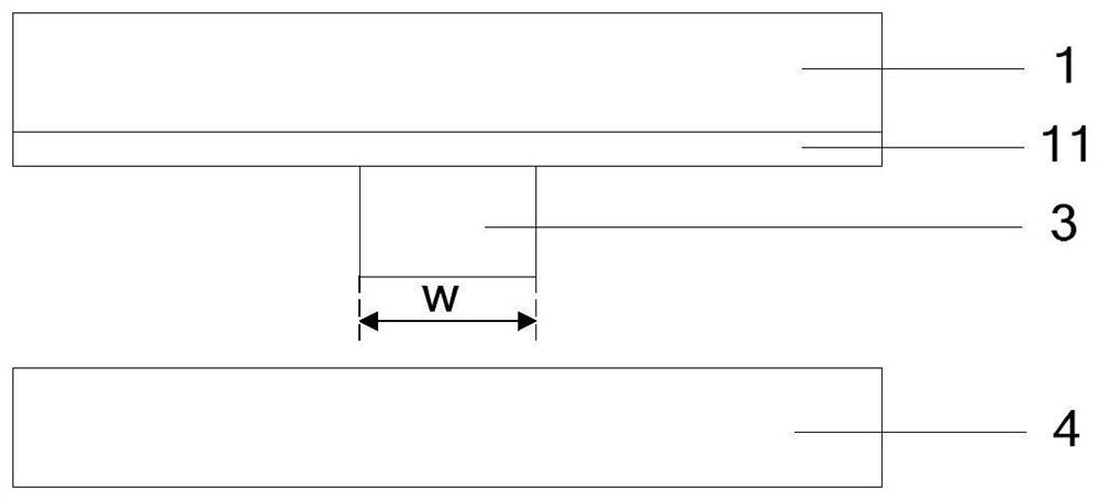
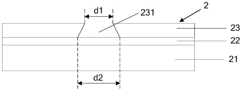
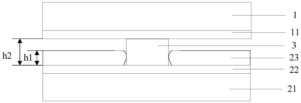
[0033] The present invention provides a micro-LED transfer method, which is used to transfer a light-emitting element to an array substrate by using a transfer substrate. In an embodiment of the present invention, the light-emitting element is a micro-LED.

[0034] The following combination Figure 1 to Figure 5 , describe in detail the micro-LED transfer printing method of the present invention, such as Figure 1 to Figure 5 As shown, the method includes the following steps:

[0035] St...


PUM


Abstract

The invention provides a micro-light emitting diode transfer printing method and an array substrate. By forming a photoresist pattern including an opening with a small top and a large bottom on the organic layer of the array substrate, the size of the upper edge of the opening is smaller than or equal to that to be transferred. In this way, after the transfer substrate carrying the light-emitting element to be transferred is aligned with the array substrate, the light-emitting element to be transferred can be firmly engaged in the opening by applying pressure to the transfer substrate, Thereby increasing the adhesion of the light-emitting elements to be transferred on the array substrate, reducing the risk of the light-emitting elements to be transferred being taken away by the transfer substrate during the process of removing the transfer substrate, increasing the transfer success rate and improving product yield , to avoid bad dark spots.

Description

technical field [0001] The invention relates to the field of display technology, in particular to a micro light emitting diode transfer printing method and an array substrate. Background technique [0002] Micro LED (miniature light-emitting diode) is to make the LED structure thinner, miniaturized, and arrayed, and its size is only about 1-10 μm. Micro LED panels can be prepared using a transfer process, that is, Thin Film Transfer (thin film transfer) process. Specifically, firstly, a Micro LED epitaxial thin film structure of micron scale is formed, and a temporary substrate (ie transfer substrate) is used to carry the LED epitaxial thin film structure. Then, according to the required pixel pitch on the driving circuit substrate, the Micro LED epitaxial thin film structure is transferred in batches by using the transfer substrate, so that it is bonded to the driving circuit substrate (ie, the array substrate) to form pixels. [0003] However, when the existing transfer ...

Claims


Application Information

Patent Timeline
Patent Type & Authority Patents(China)
IPC IPC(8): G03F7/00G03F7/004
CPCG03F7/0002G03F7/004
Inventor 邹祥祥何晓龙
Owner BOE TECH GRP CO LTD
Why Eureka
Try Eureka