

Grid electrode driving circuit and driving method thereof and display device
A gate drive circuit and gate technology, applied in static indicators, instruments, etc., can solve problems such as poor display and drift of TFT electrical characteristics, and achieve the effects of reducing poor display, inhibiting threshold voltage drift, and reducing time
- Summary
- Abstract
- Description
- Claims
- Application Information
AI Technical Summary
Problems solved by technology
Method used
Image

Examples
Embodiment 1
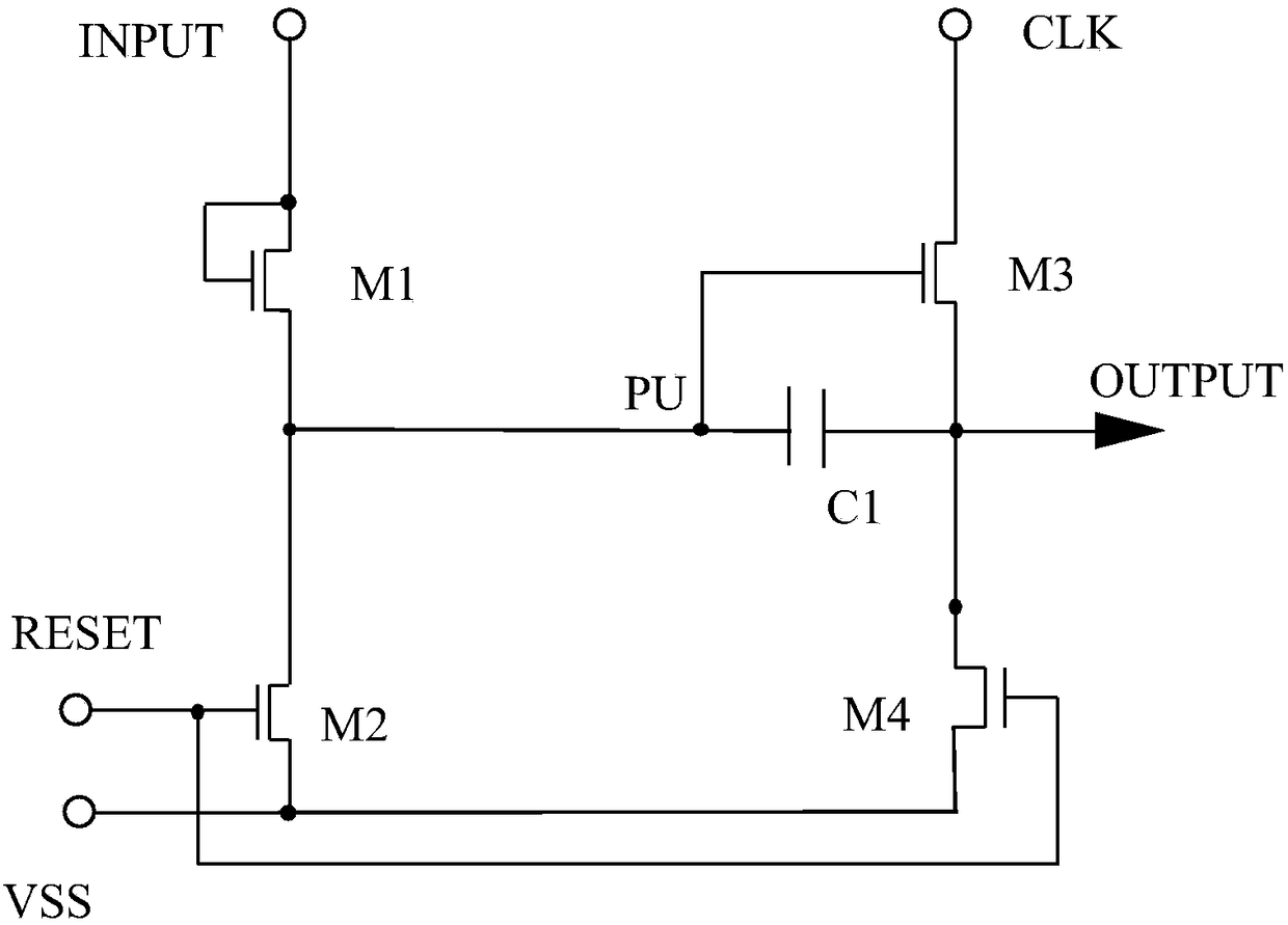
[0059] refer to image 3 , shows a schematic diagram of a gate driving circuit provided by Embodiment 1 of the present invention.
[0060] The gate drive circuit includes: an input module 1 , a first pull-up module 2 , a second pull-up module 3 , a first pull-down module 4 , a second pull-down module 5 , a reset module 6 and a storage module 7 .
[0061] The input module 1 is respectively connected to the input signal terminal INPUT and the pull-up node PU.
[0062] The first pull-up module 2 is respectively connected to the first control signal terminal CtrlA, the pull-up node PU, the first clock signal terminal CLK and the output terminal OUTPUT, and is used to output a high level to the output terminal OUTPUT under the control of the first control signal .
[0063] The second pull-up module 3 is respectively connected to the second control signal terminal CtrlB, the pull-up node PU, the first clock signal terminal CLK and the output terminal OUTPUT, for outputting a high ...
Embodiment 2
[0099] refer to Figure 6 , shows a schematic diagram of a gate driving circuit provided by Embodiment 2 of the present invention.
[0100] exist image 3 On the basis of , the gate drive circuit also includes a pull-down control module 8 and a third pull-down module 9 .
[0101] The pull-down control module 8 is respectively connected with the second clock signal terminal CLKB, the pull-down node PD, the pull-up node PU and the first level signal terminal VSS, and is used to pull down the level of the pull-down node PD under the control of the second clock signal; The second clock signal and the first clock signal input from the first clock signal terminal CLK are mutually same-frequency and anti-phase signals.
[0102] The third pull-down module 9 is respectively connected to the pull-down node PD, the first level signal terminal VSS, the pull-up node PU and the output terminal OUTPUT, and is used to pull down the levels of the pull-up node PU and the output terminal OUTPU...
PUM
 Abstract
Description
Claims
Application Information