Chip integrated boiling enhancement heat exchange structure and preparation method thereof based on MEMS (Micro Electro Mechanical System) technology

A technology for strengthening heat exchange and chips, applied in electrical components, electric solid devices, circuits, etc., can solve problems such as dry burning, and achieve the effect of strengthening heat dissipation, boiling heat exchange, and bubble detachment efficiency.

Active Publication Date: 2018-06-29
SHANGHAI JIAO TONG UNIV
View PDF6 Cites 1 Cited by
  • Summary
  • Abstract
  • Description
  • Claims
  • Application Information

AI Technical Summary

Problems solved by technology

However, this structure also has certain limitations under high heat flux density, and the large bubbles generated are not easy to detach from the surface, facing the problem of dry burning

Method used


Image

  • Chip integrated boiling enhancement heat exchange structure and preparation method thereof based on MEMS (Micro Electro Mechanical System) technology
  • Chip integrated boiling enhancement heat exchange structure and preparation method thereof based on MEMS (Micro Electro Mechanical System) technology
  • Chip integrated boiling enhancement heat exchange structure and preparation method thereof based on MEMS (Micro Electro Mechanical System) technology

Examples


Embodiment 1

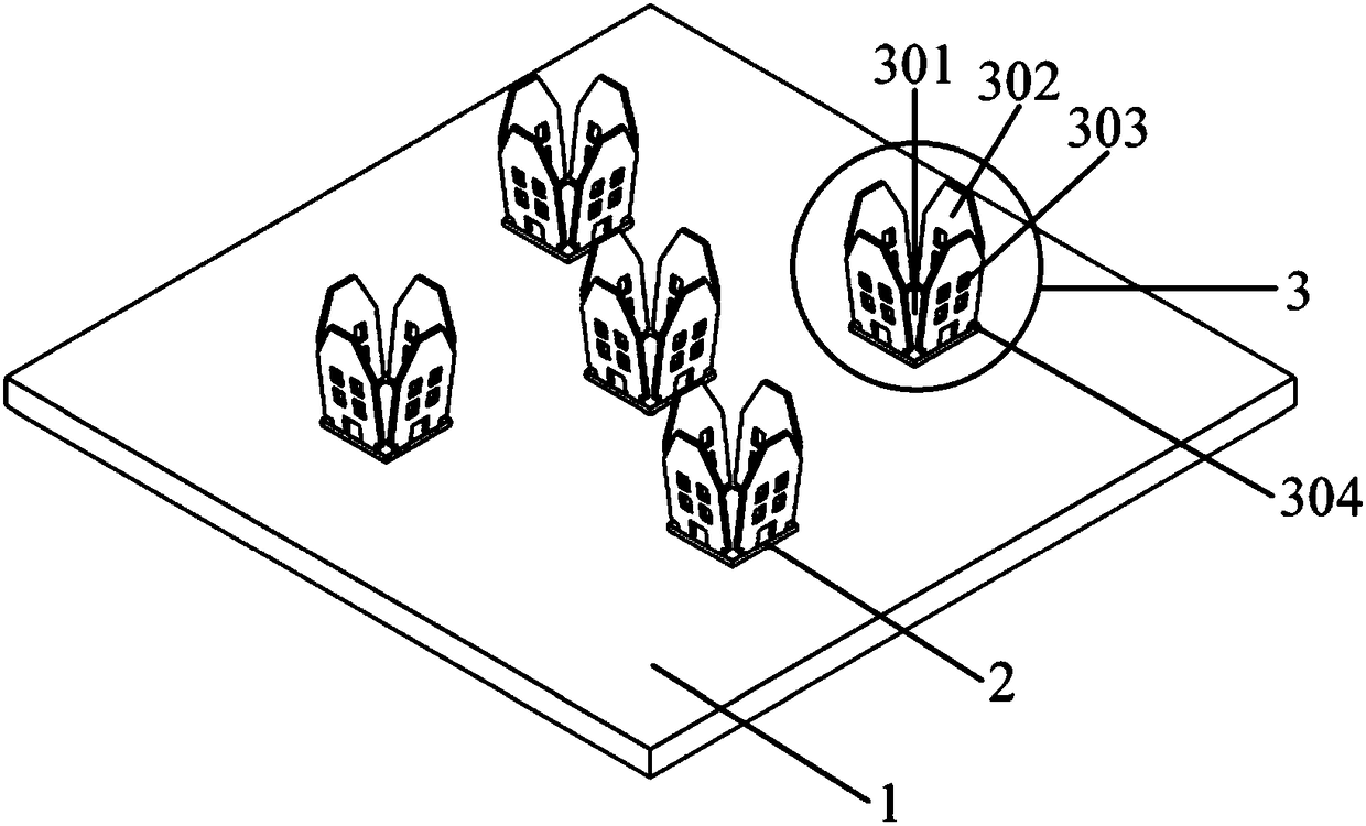
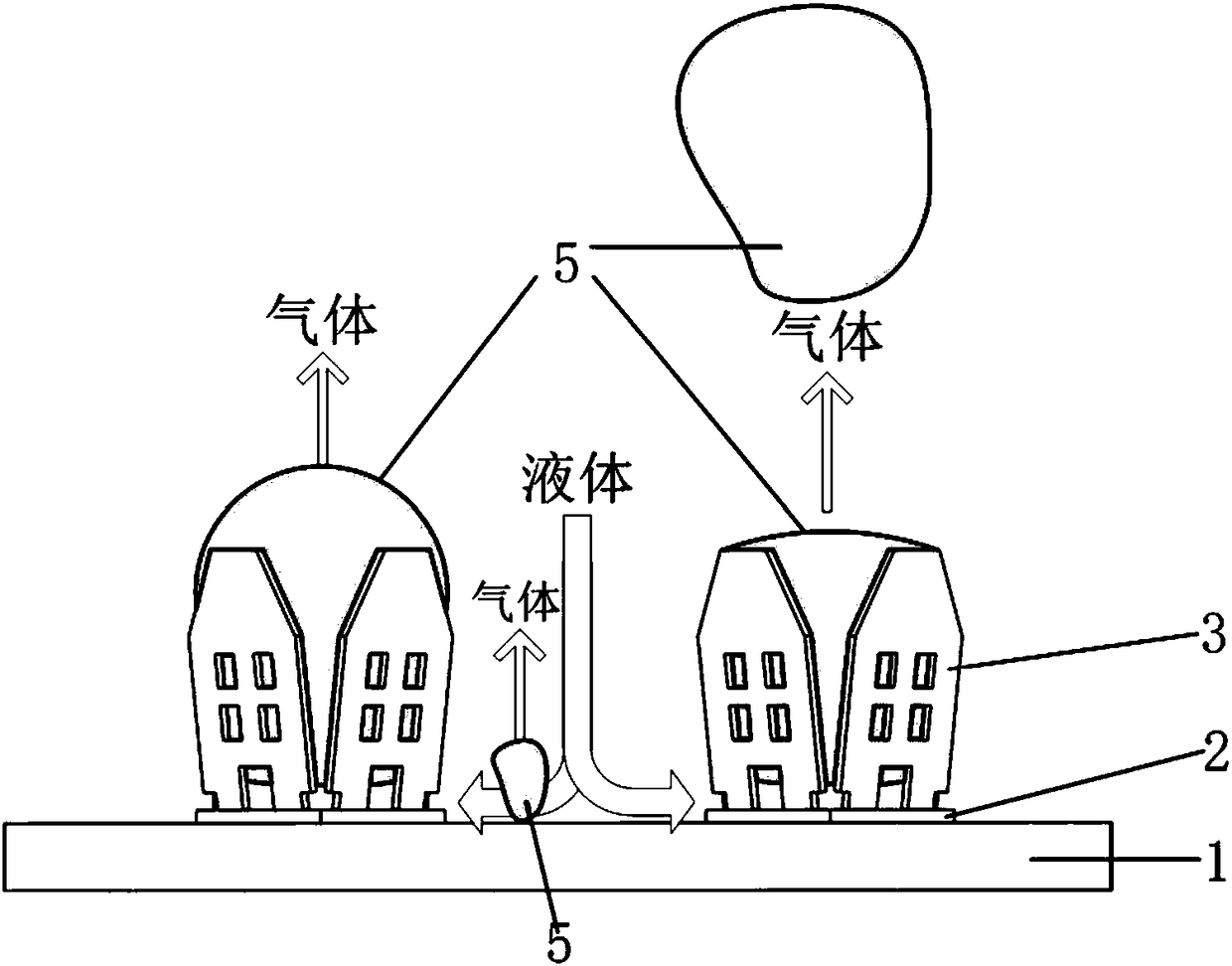
[0055] Such as figure 1 As shown, this embodiment provides a chip-integrated boiling-enhanced heat transfer structure based on MEMS technology, including: a heat-conducting substrate 1, a support layer 2, and a claw-shaped structure 3, wherein:

[0056] The heat-conducting substrate 1 is made of AlN material, and the support layer 2 and the claw structure 3 are made of copper material.

[0057] The support layer 2 is evenly distributed on the surface of the heat-conducting substrate 1, and the bottom heat-conducting metal layer 301 of each claw structure 3 is connected and fixed to the support layer 2;

[0058] The claw-shaped structure 3 is composed of a bottom heat-conducting metal layer 301 and a plurality of sidewall metal sheets 302, the bottom heat-conducting metal layer 301 is arranged on the support layer 2, and one end of the plurality of sidewall metal sheets 302 is fixed On the bottom heat-conducting metal layer 301 , the other ends of the plurality of sidewall met...

Embodiment 2

[0073] Such as Figure 4 As shown, this embodiment provides a chip-integrated boiling-enhanced heat transfer structure based on MEMS technology. Compared with Embodiment 1, this embodiment changes the material of the heat-conducting substrate and the size and distribution density of the claw structure. Specifically, the chip integrated boiling enhanced heat transfer structure includes: a thermally conductive substrate 1, a support layer 2, and a claw structure 3, wherein:

[0074] The heat-conducting substrate 1 is cut from a silicon wafer, and the support layer 2 and the claw structure 3 are both made of copper. The support layer 2 is evenly distributed on the surface of the heat conduction substrate 1, and the bottom heat conduction metal layer 301 of each claw structure 3 is connected and fixed to the copper support layer 2; the side wall metal layer of the claw structure 3 The sheet 302 has holes 303, and gaps are left between the sidewall metal sheets 302 to ensure the l...

Embodiment 3

[0081] Such as Figure 5 As shown, the appearance of the chip-integrated boiling-enhanced heat transfer structure based on MEMS technology provided by this embodiment is the same as that of Embodiment 1, including: a thermally conductive substrate 1, a support layer 2, and a claw-shaped structure 3, wherein:

[0082] The heat-conducting substrate 1 is made of AlN material, and the support layer 2 and the claw structure 3 are made of copper material. The structure and size of each component of the chip integrated boiling enhancement are also the same as those in Example 1.

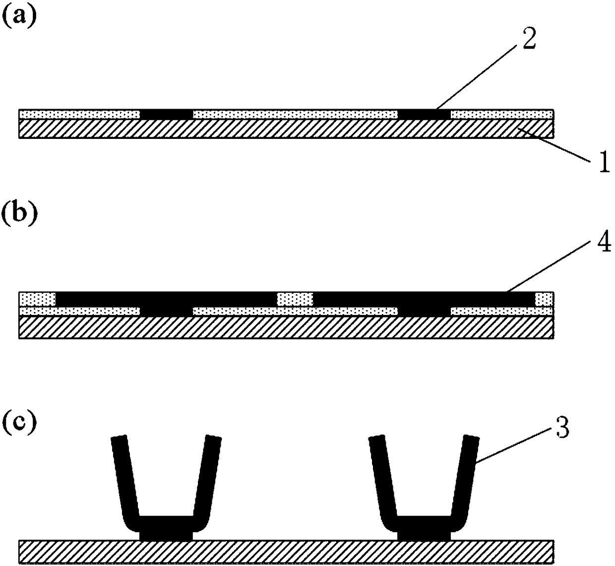
[0083] Different from Embodiments 1 and 2, in this embodiment, a patterned layer is added to the chip-integrated boiling enhanced heat transfer structure process to make micropores on the inner wall of the claw-shaped structure 3 and increase the nucleation sites there. Such as Figure 5 As shown, in this embodiment, the overall processing flow of the boiling enhanced heat transfer structure is as follows...


PUM


Abstract

The invention provides a chip integrated boiling enhancement heat exchange structure and a preparation method thereof based on an MEMS (Micro Electro Mechanical System) technology. The chip integratedboiling enhancement heat exchange structure comprises a heat conducting substrate, wherein a supporting layer is arranged on the surface of the heat conducting substrate; a plurality of claw type structures are arranged on the supporting layer; the claw type structures are obtained by preparing suspended metal sheet structures by adopting a surface micro-machining method, and folding the suspended metal sheet structures along plane normal thereof. According to the chip integrated boiling enhancement heat exchange structure disclosed by the invention, a path of combining and growing a large amount of surface bubbles into an air film is blocked off by the array claw type structures, so that the dry burning risk is avoided; porous structures can be prepared in the side walls of the claw typestructures so as to ensure liquid supply below the bubbles in the cavity and intensify the separating efficiency of the bubbles; the effects of increasing the heat exchange area by the claw type structures and further intensifying heat exchange by using bubble turbulence and convection of the metal side wall can be realized. Besides, the designed substrate material and a processing mode are derived from a chip integration technology, and application of the structure in integrated heat dissipation of electronic devices is favorably realized.

Description

technical field [0001] The invention relates to the technical field of high heat flux boiling enhanced heat transfer, in particular to a chip-integrated boiling enhanced heat transfer structure based on MEMS technology and a preparation method thereof. Background technique [0002] With the rapid development of science and technology, the high density and miniaturization of electronic devices has become an inevitable trend, and the calorific value per unit volume continues to increase, making heat dissipation of high-power devices an urgent problem to be solved. Boiling heat transfer is a phase-change heat transfer method. Compared with traditional air cooling and liquid convection heat transfer, the heat transfer coefficient has an order of magnitude difference, and it is a very effective heat dissipation method. However, the heat transfer performance of boiling with high heat flux is often seriously deteriorated. The fundamental reason is that the bubbles generated by boil...

Claims


Application Information

Patent Timeline
Patent Type & Authority Applications(China)
IPC IPC(8): H01L23/367H01L23/46
CPCH01L23/367H01L23/46
Inventor 常昕悦王艳金之钰丁桂甫
Owner SHANGHAI JIAO TONG UNIV
Why Eureka
Try Eureka