Chip oxygen sensor and preparation method thereof
The technology of an oxygen sensor and a manufacturing method, which is applied in the field of oxygen sensors, can solve the problems of poor flexural strength of the sheet-type oxygen sensor, prone to cracks and warpage, complicated manufacturing process, etc., achieves easy printing and uniformity, and is beneficial to industrialized production and preparation. simple craftsmanship
- Summary
- Abstract
- Description
- Claims
- Application Information
AI Technical Summary
Problems solved by technology
Method used
Image
Examples
Embodiment 2
[0033] Embodiment 2 of the manufacturing method of the chip oxygen sensor, the steps are as follows:
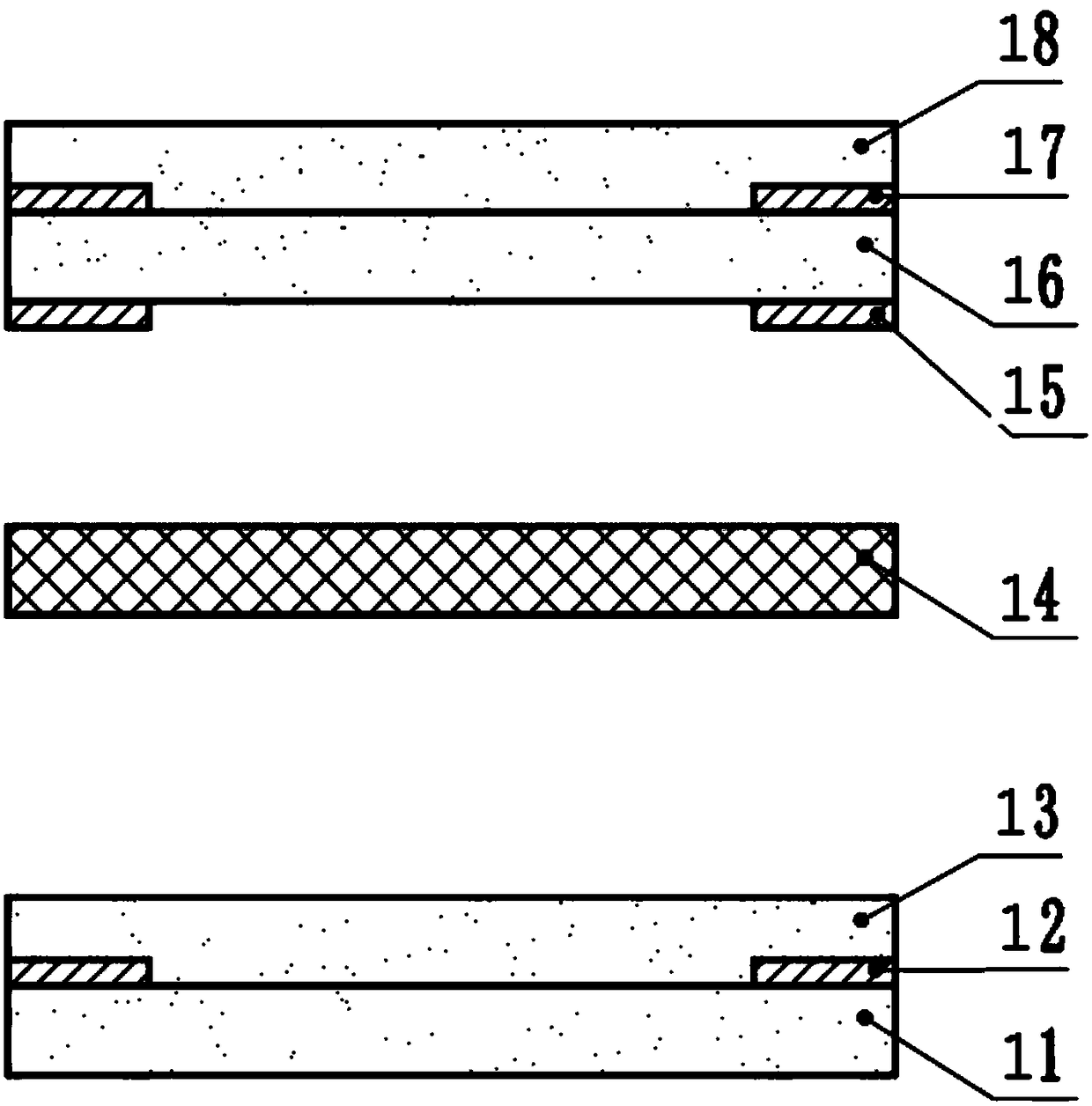
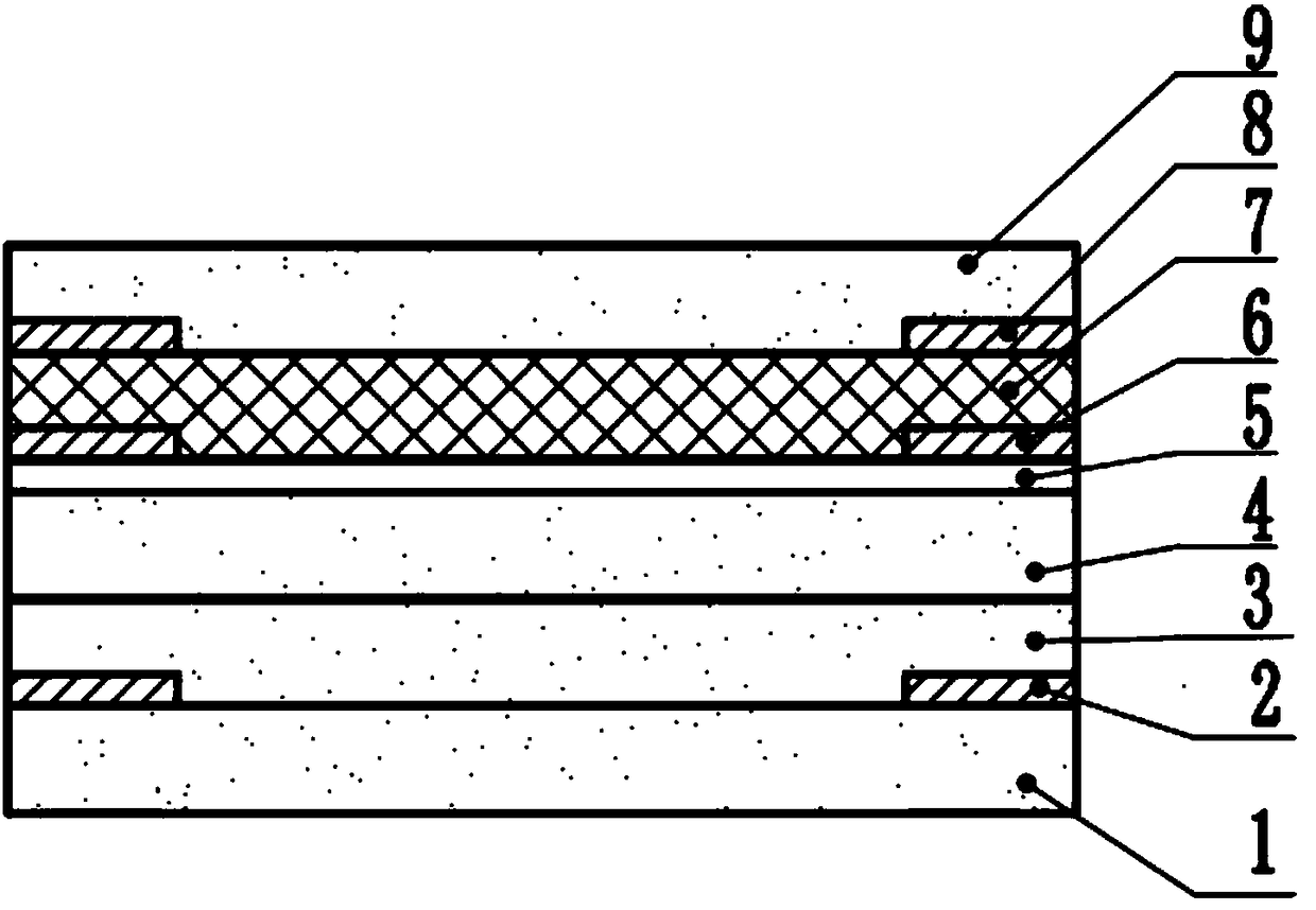
[0034] The alumina ceramic substrate 4 that has been sintered into a dense body with a purity of 80% and a thickness of 0.5 mm is prepared, and the first insulating layer 3 is printed on one side of the ceramic substrate 4. The wet film thickness of the first insulating layer 3 printed is 30um, dry, then print the heating electrode 2, the wet film thickness printed on the heating electrode 2 is 20um, dry, then print the second insulating layer 1, the wet film thickness printed on the second insulating layer 1 is 30um, dry , and then sintering the ceramic substrate 4 at a high temperature of 1500° C. to form a heater base.
[0035] Continue to print the third insulating layer 5 on the same side of the ceramic substrate 4, the wet film thickness of the third insulating layer 5 printing is 30um, dry, and then print the first porous platinum electrode 6, and the first porous plat...
Embodiment 3
[0037] Embodiment 3 of the manufacturing method of the chip oxygen sensor, the steps are as follows:
[0038] The alumina ceramic substrate 4 that has been sintered into a dense body with a purity of 93% and a thickness of 0.635 mm is prepared, and the first insulating layer 3 is printed on one side of the ceramic substrate 4. The wet film thickness of the first insulating layer 3 printed is 80um, dry, then print the heating electrode 2, the wet film thickness printed on the heating electrode 2 is 60um, dry, then print the second insulating layer 1, the wet film thickness printed on the second insulating layer 1 is 100um, dry .
[0039] Print the third insulating layer 5 on the other side of the ceramic substrate 4, the wet film thickness of the third insulating layer 5 printing is 80um, dry, then print the first porous platinum electrode 6, the first porous platinum electrode 6 printing The wet film thickness is 60um, dry, and then print the reference layer 7, the wet film t...
PUM
| Property | Measurement | Unit |
|---|---|---|
| purity | aaaaa | aaaaa |
Abstract
Description
Claims
Application Information

