MRAM chip and storage unit reading method thereof

A storage unit and chip technology, applied in information storage, static memory, digital memory information, etc., can solve the problems of small ratio, not easy to read errors, difficult to greatly improve the magnetoresistance, and reduce reading errors. possibility, increase the number of effective memory cells, and avoid the effect of small signal difference

Active Publication Date: 2018-07-06
SHANGHAI CIYU INFORMATION TECH
View PDF5 Cites 11 Cited by
  • Summary
  • Abstract
  • Description
  • Claims
  • Application Information

AI Technical Summary

Problems solved by technology

[0007] However, with the increase of the capacity of the magnetic random access memory and the reduction of the size of the MRAM storage unit, it is limited by the manufacturing process. On the one hand, it is difficult to greatly increase the magnetoresistivity, and on the other hand, the resistance standard deviation of the MRAM storage unit is increasing. In particular, the standard deviation of the high-impedance state increases even more
This makes the tails of the two distributions in the double-bell curve longer and longer, and the distance between the low-resistance tail of the high-resistance distribution and the high-resistance tail of the low-resistance distribution is getting smaller and smaller from the midpoint reference resistance, which also leads to More detected MRAM memory cells are less likely to be read by the reference resistor to distinguish the resistance state and generate read errors
[0008] Another serious disadvantage is that due to the asymmetry of the double bell curve, the standard deviation of the reference resistance of the high-resistance state of the MRAM memory cell is much larger than that of the reference resistance of the low-resistance state. If the reference resistance is the midpoint resistance, the MRAM storage The ratio of the signal difference between the high resistance value of the cell and the reference resistance to the standard deviation of the high state resistance will be much smaller than that of the low resistance state.

Method used


Image

  • MRAM chip and storage unit reading method thereof
  • MRAM chip and storage unit reading method thereof
  • MRAM chip and storage unit reading method thereof

Examples


Embodiment Construction

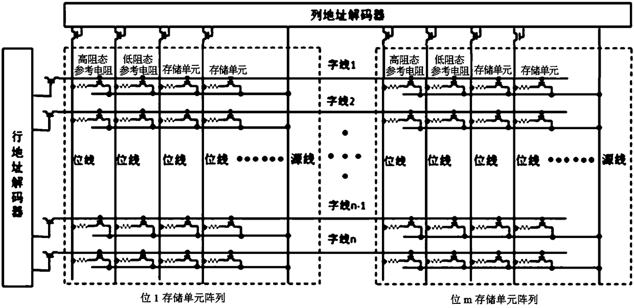
[0046] Such as figure 2 As shown, the MRAM chip of an embodiment of the present invention includes a plurality of array groups, and each array group includes m arrays composed of MRAM memory cells, and m bits in a word are respectively stored in m arrays in the array group For the MRAM memory cells at the same position, each array also includes a low-resistance state reference resistor column and a high-resistance state reference resistor column.

[0047] The MRAM memory cells in the same row in each array share the low-resistance state reference resistor and the high-resistance state reference resistor in the same row.

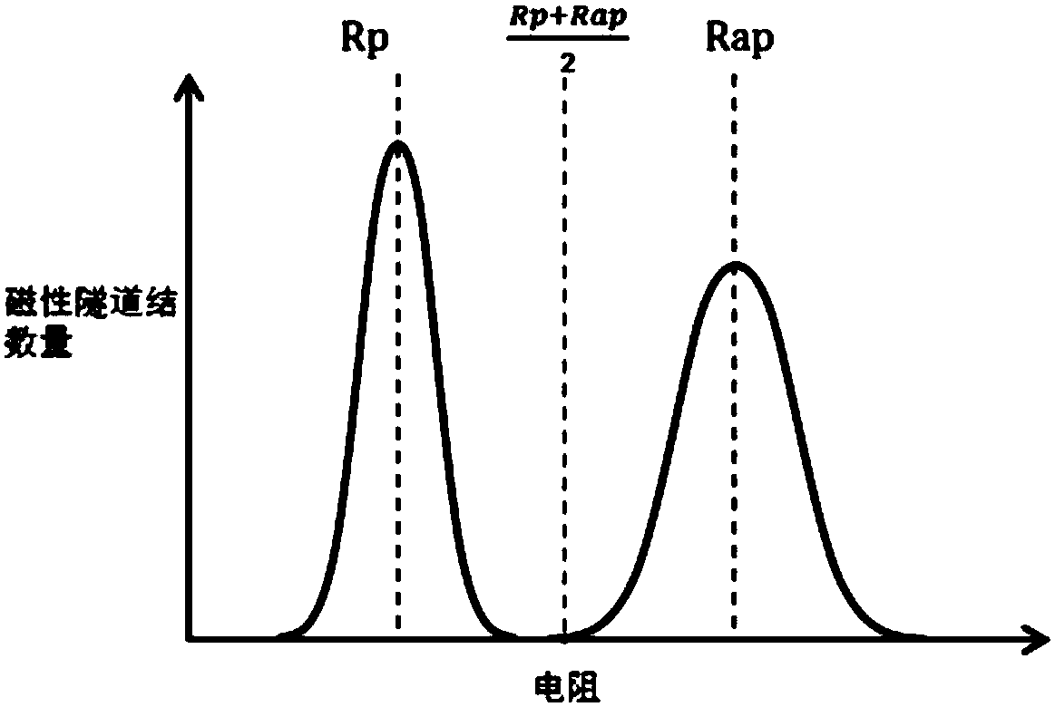
[0048] On the one hand, since the m bits in a word are respectively stored in the MRAM memory cells in the same position of the m arrays in the array group, the reference resistors are arranged in an array containing only one bit, so that the memory cells sharing the same reference resistor The number is reduced, so the standard deviation is reduced, which ...


PUM


Abstract

The invention provides am MRAM chip. The MRAM chip comprises a plurality of array groups, wherein each array group comprises m arrays; m bits in a word are respectively stored in the m arrays; and each array comprises a low-resistance state reference resistor column and a high-resistance state reference resistor column. The invention furthermore provides a storage unit reading method. According tothe MRAM chip and the storage unit reading method, the m bits of the word are respectively stored in the m arrays, and reference resistors are arranged in arrays which only comprise one bit, respectively, so that the number of storage units which share a same reference resistor is decreased, the standard difference is decreased, and the problem of high reading error rate caused by relatively small signal difference is avoided; each array only comprises two columns of reference resistors, so that the numbers of the reference resistors and the storage units are relatively small, and the numberof effective storage units in a unit area can be increased; and by adopting cross stepwise superposition to obtain signals and adjust weights, the reference resistors can have optimum values and the reading error probability is decreased.

Description

technical field [0001] The invention relates to the field of memory of semiconductor chips, in particular to an MRAM chip and a method for reading memory units thereof. Background technique [0002] Magnetic Random Access Memory (MRAM) is an emerging non-volatile storage technology. It has high-speed read and write speed and high integration, and can be rewritten infinitely. [0003] An MRAM is composed of an array of magnetoresistive memory cells. Each magnetoresistive memory unit contains a structure called MRAM memory unit (Magnetic Tunnel Junction, MTJ). An MRAM memory cell consists of two layers of ferromagnetic material sandwiching a very thin layer of non-ferromagnetic insulating material. One layer of ferromagnetic material is a reference layer with a fixed magnetization direction, and the other layer of ferromagnetic material is a memory layer with a variable magnetization direction, and its magnetization direction can be parallel or antiparallel to the fixed mag...

Claims


Application Information

Patent Timeline
Patent Type & Authority Applications(China)
IPC IPC(8): G11C11/16
CPCG11C11/1673
Inventor 俞华樑
Owner SHANGHAI CIYU INFORMATION TECH
Why Eureka
Try Eureka