TFT manufacturing method and TFT substrate

A manufacturing method and substrate substrate technology, applied in semiconductor/solid-state device manufacturing, electrical components, electrical solid-state devices, etc., can solve problems affecting the characteristics of TFT devices, etc., and achieve the effect of avoiding etching residues

Inactive Publication Date: 2018-07-06
WUHAN CHINA STAR OPTOELECTRONICS SEMICON DISPLAY TECH CO LTD
View PDF4 Cites 1 Cited by
  • Summary
  • Abstract
  • Description
  • Claims
  • Application Information

AI Technical Summary

Problems solved by technology

In the subsequent dry etching (Dry etch) process, the photoresist pattern 12 covers the part of the polysilicon layer 11 that needs to be preserved, and exposes the part that needs to be etched and removed, but the protrusion 111 that is not covered by the photoresist pattern 12 is very small. It is difficult to be completely etched and removed, resulting in the polysilicon residue 112 on the substrate 10, that is, the etching residue, which seriously affects the characteristics of the TFT device

Method used


Image

  • TFT manufacturing method and TFT substrate
  • TFT manufacturing method and TFT substrate
  • TFT manufacturing method and TFT substrate

Examples


Embodiment Construction

[0047] The following will clearly and completely describe the technical solutions of each exemplary embodiment provided by the present invention with reference to the accompanying drawings in the embodiments of the present invention. In the case of no conflict, the following embodiments and features in the embodiments can be combined with each other.

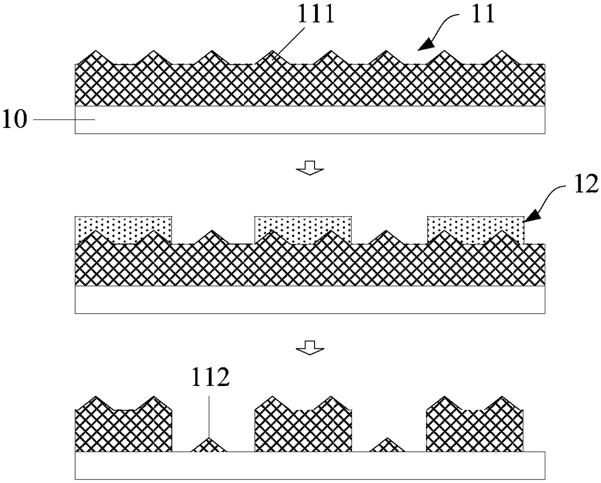
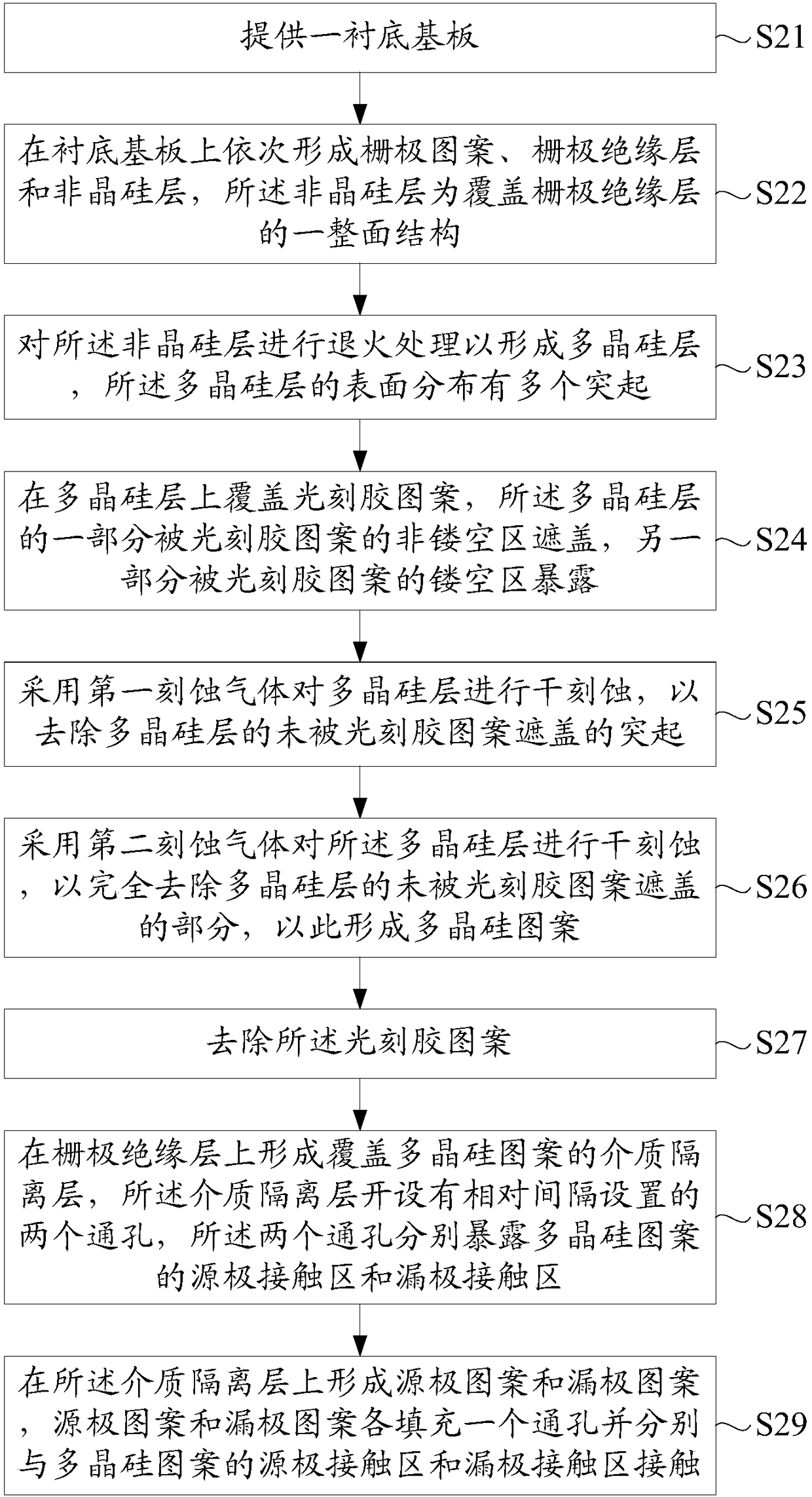
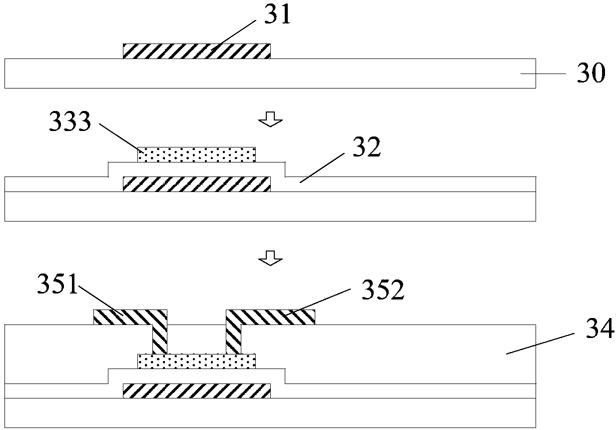
[0048] figure 2 It is a schematic flow chart of a manufacturing method of a TFT according to an embodiment of the present invention, image 3 is based on figure 2 Schematic diagram of the scenario of TFT fabrication by the shown method. combine figure 2 and image 3 As shown, the manufacturing method of the TFT includes the following steps S21-S29.

[0049] S21: Provide a base substrate.

[0050] The base substrate 30 may be a transparent substrate such as a glass substrate, a plastic substrate, or a flexible substrate.

[0051] S22: sequentially forming a gate pattern, a gate insulating layer and an amorphous silicon ...


PUM


Abstract

The invention discloses a TFT manufacturing method and a TFT substrate. In the process of etching to form a polysilicon pattern, one part of a polysilicon layer is covered by a non-hollowed region ofa photoresist pattern, the other part is exposed by a hollowed-out region of the photoresist pattern, secondly, dry etching of the polysilicon layer is carried out through employing the first etchinggas to remove protrusion of the polysilicon layer not covered by the photoresist pattern, and dry etching of the polysilicon layer is carried out through employing the second etching gas to remove thepart of the polysilicon layer not covered by the photoresist pattern. The method is advantaged in that complete etching can be facilitated to remove the polysilicon layer not covered by the photoresist pattern, and etching residue is avoided.

Description

technical field [0001] The invention relates to the field of display technology, in particular to a TFT (Thin Film Transistor, thin film transistor) manufacturing method and a TFT substrate. Background technique [0002] In the manufacturing process of TFT, such as figure 1 As shown, when the polysilicon (p-Si) layer 11 is formed by the ELA (Excimer Laser Anneal, excimer laser annealing) process on the amorphous silicon (a-Si) layer on the substrate 10, the grain boundary when adjacent crystal nuclei grow Pressing each other, after the crystallization is completed, the surface of the polysilicon layer 11 will form protrusions 111 with smaller shapes. In the subsequent dry etching (Dry etch) process, the photoresist pattern 12 covers the part of the polysilicon layer 11 that needs to be preserved, and exposes the part that needs to be etched and removed, but the protrusion 111 that is not covered by the photoresist pattern 12 is very small. It is difficult to be completely ...

Claims


Application Information

Patent Timeline
Patent Type & Authority Applications(China)
IPC IPC(8): H01L21/336H01L27/12H01L21/77
CPCH01L27/1259H01L27/127H01L29/6675
Inventor 喻蕾李松杉
Owner WUHAN CHINA STAR OPTOELECTRONICS SEMICON DISPLAY TECH CO LTD
Why Eureka
Try Eureka