A method of manufacturing an embedded flash memory gate

A production method and embedded technology, which is applied in the direction of semiconductor devices, electrical components, circuits, etc., can solve the problems of long process time and high cost, and achieve the effects of process simplification, cost saving, and photolithography steps

Active Publication Date: 2019-02-22
WUHAN XINXIN SEMICON MFG CO LTD
View PDF3 Cites 0 Cited by
  • Summary
  • Abstract
  • Description
  • Claims
  • Application Information

AI Technical Summary

Problems solved by technology

[0009] The above process forms the gate of the logic region and the select gate and erase gate of the storage region through two polysilicon depositions, silicon oxide protective layer deposition, photolithography, chemical mechanical polishing and etching. The entire process takes a long time and is expensive.

Method used


Image

  • A method of manufacturing an embedded flash memory gate
  • A method of manufacturing an embedded flash memory gate
  • A method of manufacturing an embedded flash memory gate

Examples


Embodiment Construction

[0030] In order to make the content of the present invention clearer and easier to understand, the content of the present invention will be further described below in conjunction with the accompanying drawings. Of course, the present invention is not limited to this specific embodiment, and general replacements known to those skilled in the art are also covered within the protection scope of the present invention.

[0031] Secondly, the present invention is described in detail by means of schematic diagrams. When describing the examples of the present invention in detail, for the convenience of illustration, the schematic diagrams are not partially enlarged according to the general scale, which should not be used as a limitation of the present invention.

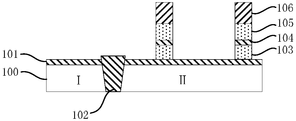
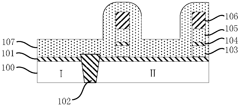
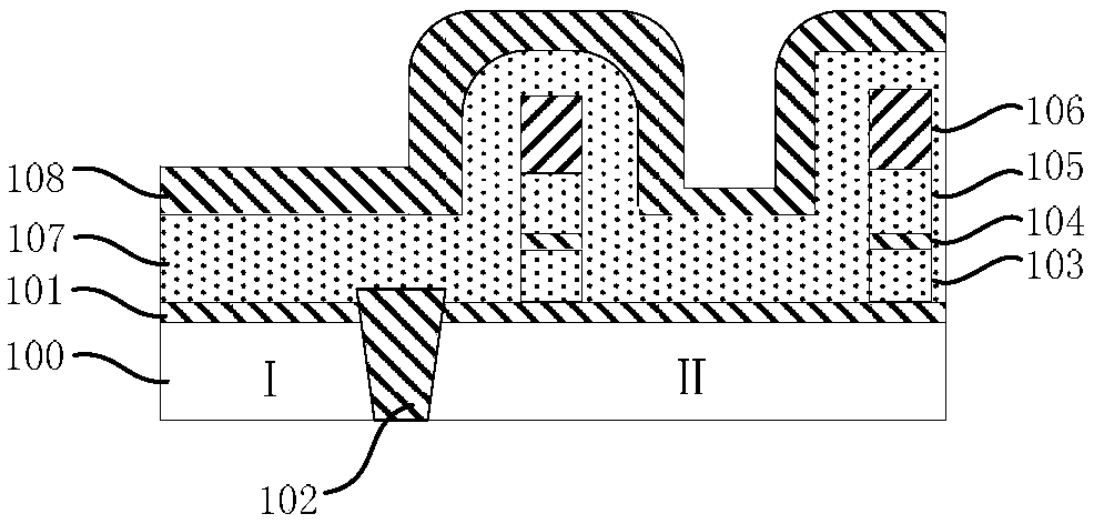
[0032] As mentioned in the background technology, in the process of manufacturing embedded flash memory gates in the prior art, in order to eliminate the step difference between the logic area and the storage area, two times ...


PUM


Abstract

The present invention provides a manufacturing method of embedded flash memory gate, comprising: providing a substrate, the substrate includes a logic area and a storage area, forming a gate oxide layer on the substrate, and forming a gate oxide layer in the storage area A floating gate, a gate dielectric layer, a control gate and a barrier layer are sequentially formed on a part of the gate oxide layer; a polysilicon layer is formed, and the polysilicon layer covers the logic region and the storage region; a protective layer is formed, and the protective layer covering the polysilicon layer, and the protection layer on the logic area is higher than the barrier layer on the storage area; performing planarization on the protection layer to expose the polysilicon layer on the storage area, and remaining part of the protective layer; using the remaining protective layer as a mask, etch the polysilicon layer on the storage area to the thickness of the remaining part of the polysilicon layer; remove the remaining protective layer. The manufacturing method of the embedded flash memory gate provided by the invention simplifies the technological process and saves the cost.

Description

technical field [0001] The invention relates to a semiconductor manufacturing process, in particular to a method for manufacturing an embedded flash gate. Background technique [0002] In the current semiconductor industry, integrated circuit products can be mainly divided into three types: analog circuits, digital circuits and digital / analog hybrid circuits, among which storage devices are an important type of digital circuits. In recent years, the development of embedded flash memory (embedded flash, Eflash) in storage devices is particularly rapid. The main feature of embedded flash memory is that it can keep stored information for a long time without power on, and has the advantages of high integration, fast access speed, easy erasing and rewriting, etc. field has been widely used. [0003] The flash storage area in the embedded flash memory device has a stacked gate structure, which includes a tunnel oxide layer, a polysilicon floating gate for storing charges, and a ...

Claims


Application Information

Patent Timeline
Patent Type & Authority Patents(China)
IPC IPC(8): H01L27/11524H01L27/11529H01L27/11531
CPCH10B41/35H10B41/42H10B41/41
Inventor 张超然李赟周俊
Owner WUHAN XINXIN SEMICON MFG CO LTD
Why Eureka
Try Eureka