A display panel and a display device

A display panel and display substrate technology, applied in semiconductor devices, electrical components, circuits, etc., can solve problems such as packaging failure, achieve the effect of improving the success rate of packaging and product yield

Active Publication Date: 2020-04-10
BOE TECH GRP CO LTD
View PDF4 Cites 0 Cited by
  • Summary
  • Abstract
  • Description
  • Claims
  • Application Information

AI Technical Summary

Problems solved by technology

[0004] The present invention provides a display panel and a display device to solve the problem in the prior art that the edge of the encapsulation layer is separated from the display substrate, causing encapsulation failure

Method used


Image

  • A display panel and a display device
  • A display panel and a display device
  • A display panel and a display device

Examples


Embodiment Construction

[0024] The following will clearly and completely describe the technical solutions in the embodiments of the present invention with reference to the accompanying drawings in the embodiments of the present invention. Obviously, the described embodiments are some of the embodiments of the present invention, but not all of them. Based on the embodiments of the present invention, all other embodiments obtained by persons of ordinary skill in the art without making creative efforts belong to the protection scope of the present invention.

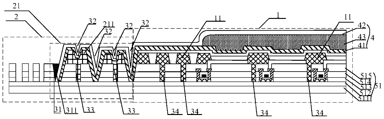
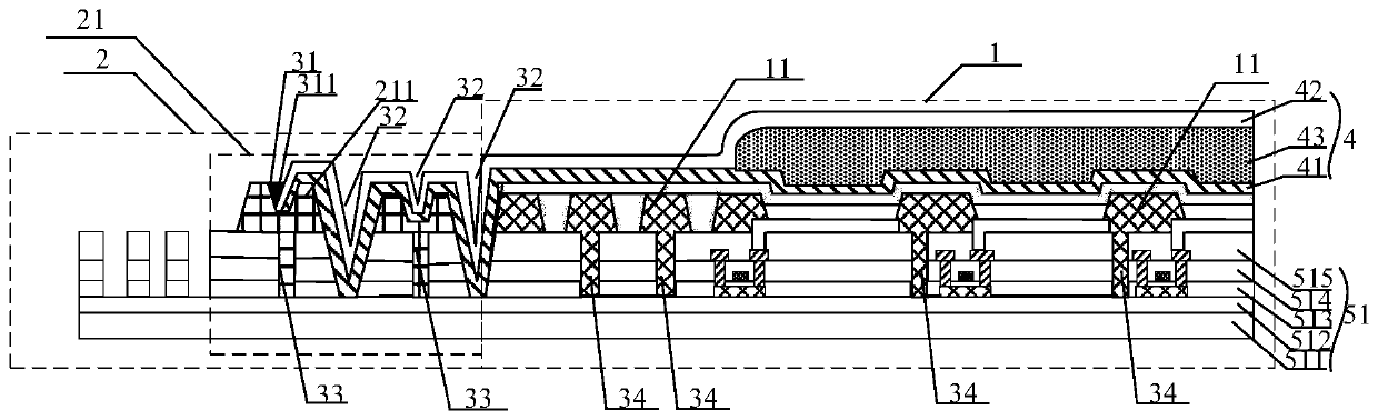
[0025] An embodiment of the present invention provides a display panel, including a display substrate and a thin film encapsulation layer encapsulated on the display substrate. The display substrate is divided into a display area and a non-display area. It can be understood that, usually, the non-display area surrounds the display area. For setting, a dam area is set in the non-display area, and the display substrate in the dam area has a first gro...


PUM


Abstract

The invention discloses a display panel and a display device. The display panel includes a display substrate and a thin film encapsulation layer encapsulated on the display substrate; the display substrate is divided into a display area and a non-display area, and the non-display area A dam area is provided, the display substrate in the dam area has a first groove, and the edge of the thin film encapsulation layer is encapsulated in the first groove. The display panel of the embodiment of the present invention includes a display substrate and a thin film encapsulation layer encapsulated on the display substrate, a first groove is provided in the coffer region of the non-display area of ​​the display substrate, and the edge of the thin film encapsulation layer is encapsulated in the first groove. In a groove, the edge of the thin film encapsulation layer is prevented from directly contacting the surface of the display substrate, thereby preventing the thin film encapsulation layer from being separated from the display substrate during the cutting or bending process of the display panel. While improving the packaging success rate, it is also conducive to improving the product yield.

Description

technical field [0001] The present invention relates to the field of display technology, in particular to a display panel and a display device. Background technique [0002] During the process of preparing quantum dot light emitting (Quantum Dot Light Emitting Diodes, QLED) devices or organic electroluminescent (Organic Light Emitting Diode, OLED) devices, cracks are prone to appear on the display device during the cutting process, and some cracks will further Diffusion to the side close to the display area causes separation of the edge of the encapsulation layer from the display substrate, causing encapsulation failure, and further resulting in poor display. [0003] In the prior art, in order to prevent cracks generated by cutting from spreading to the display area and causing package failure, grooves 1' are usually prepared in the peripheral area of ​​the display panel, such as figure 1 As shown, however, these grooves cannot completely prevent cracks from propagating to...

Claims


Application Information

Patent Timeline
Patent Type & Authority Patents(China)
IPC IPC(8): H01L51/52
CPCH10K50/84H10K59/124
Inventor 张玉欣乔勇卢永春
Owner BOE TECH GRP CO LTD
Why Eureka
Try Eureka