Display substrate and manufacturing method thereof, and display device

A technology for displaying substrates and manufacturing methods, which is applied in semiconductor/solid-state device manufacturing, electrical components, electric solid-state devices, etc., can solve problems such as different thicknesses, improve uniformity, reduce the probability of thin edges and thick edges in the middle, and ensure The effect of flatness

Inactive Publication Date: 2018-07-06
BOE TECH GRP CO LTD +1
View PDF4 Cites 14 Cited by
  • Summary
  • Abstract
  • Description
  • Claims
  • Application Information

AI Technical Summary

Problems solved by technology

In the current production, the thickness of the functional film layer around the sub-pixel area and the middle part of the sub-pixel area are different due to the different evaporation rates of the organic solution in the sub-pixel area, which causes the coffee ring effect, which is a technical problem for inkjet printing OLEDs.

Method used


Image

  • Display substrate and manufacturing method thereof, and display device
  • Display substrate and manufacturing method thereof, and display device
  • Display substrate and manufacturing method thereof, and display device

Examples


Embodiment Construction

[0037] In order to make the technical problems, technical solutions and advantages to be solved by the embodiments of the present invention clearer, the following will describe in detail with reference to the drawings and specific embodiments.

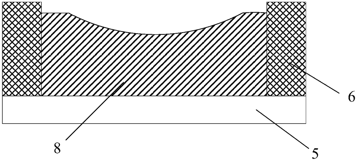
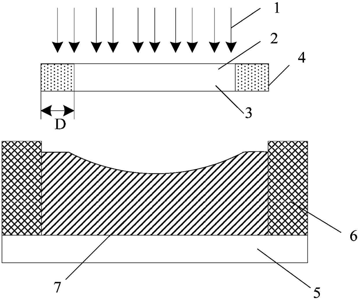
[0038] The formation of droplets in the inkjet printing process includes the process of droplet falling, spreading, and drying. After the droplet falls, the vapor pressure at the edge of the droplet is small, resulting in a faster evaporation rate of the solvent at the edge of the droplet, and the final solute is constantly in contact. The phenomenon that the thickness of the functional film layer at the peripheral part of the sub-pixel area deposited on the line is relatively large, and the thickness of the functional film layer at the middle part of the sub-pixel area is small, such as figure 1 This phenomenon is called the coffee ring effect. The coffee ring effect will make it difficult to ensure the flatness of the functional film...


PUM

PropertyMeasurementUnit
transmittivityaaaaaaaaaa

Abstract

The invention provides a display substrate and a manufacturing method thereof, and a display device, which belong to the technical field of display. The manufacturing method of the display substrate comprises a step of printing organic solution in a sub-pixel region defined by a pixel definition layer to prepare a functional film layer. The step comprises the following sub steps: printing organicsolution in the sub-pixel region; and heating and drying the organic solution, and making the evaporation rate of the solvent in the edge portion of the sub-pixel region lower than the evaporation rate of the solvent in the middle portion of the sub-pixel region during heating and drying. Through the technical scheme of the invention, a functional film layer with uniform thickness can be formed inthe sub-pixel region, and the coffee ring effect is avoided.

Description

technical field [0001] The present invention relates to the field of display technology, in particular to a display substrate, a manufacturing method thereof, and a display device. Background technique [0002] The current production of large-size OLED (organic electroluminescent diode) display products adopts the method of vacuum thermal evaporation, which has low material utilization rate and difficulty in improving yield rate, resulting in high prices of OLED display products. In order to improve material utilization and reduce costs, inkjet printing is currently being developed to produce OLED display products. [0003] The method of inkjet printing to produce OLED display products is to print an organic solution in the sub-pixel area and form a functional film layer after drying. In the current production, the thickness of the functional film layer around and in the middle of the sub-pixel area is different due to the difference in evaporation rate of the organic solut...

Claims


Application Information

Patent Timeline
Patent Type & Authority Applications(China)
IPC IPC(8): H01L51/56H01L27/32
CPCH10K59/121H10K71/135H10K71/421
Inventor 谢学武艾雨
Owner BOE TECH GRP CO LTD
Why Eureka
Try Eureka