Carrier transmission material, carrier transmission layer and organic light-emitting device

A technology of organic light-emitting devices and electron transport materials, applied in the field of organic light-emitting displays, to achieve good thermal stability and improve luminous efficiency

Active Publication Date: 2018-07-10
KUNSHAN GO VISIONOX OPTO ELECTRONICS CO LTD +1
View PDF4 Cites 19 Cited by
  • Summary
  • Abstract
  • Description
  • Claims
  • Application Information

AI Technical Summary

Problems solved by technology

[0005] Based on this, it is necessary to focus on the triplet state energy level T of carrier transport materials in existing organic light-emitting devices. 1 lower issue, providing a triplet energy level T 1 High carrier transport material

Method used


Image

  • Carrier transmission material, carrier transmission layer and organic light-emitting device
  • Carrier transmission material, carrier transmission layer and organic light-emitting device
  • Carrier transmission material, carrier transmission layer and organic light-emitting device

Examples


Embodiment approach

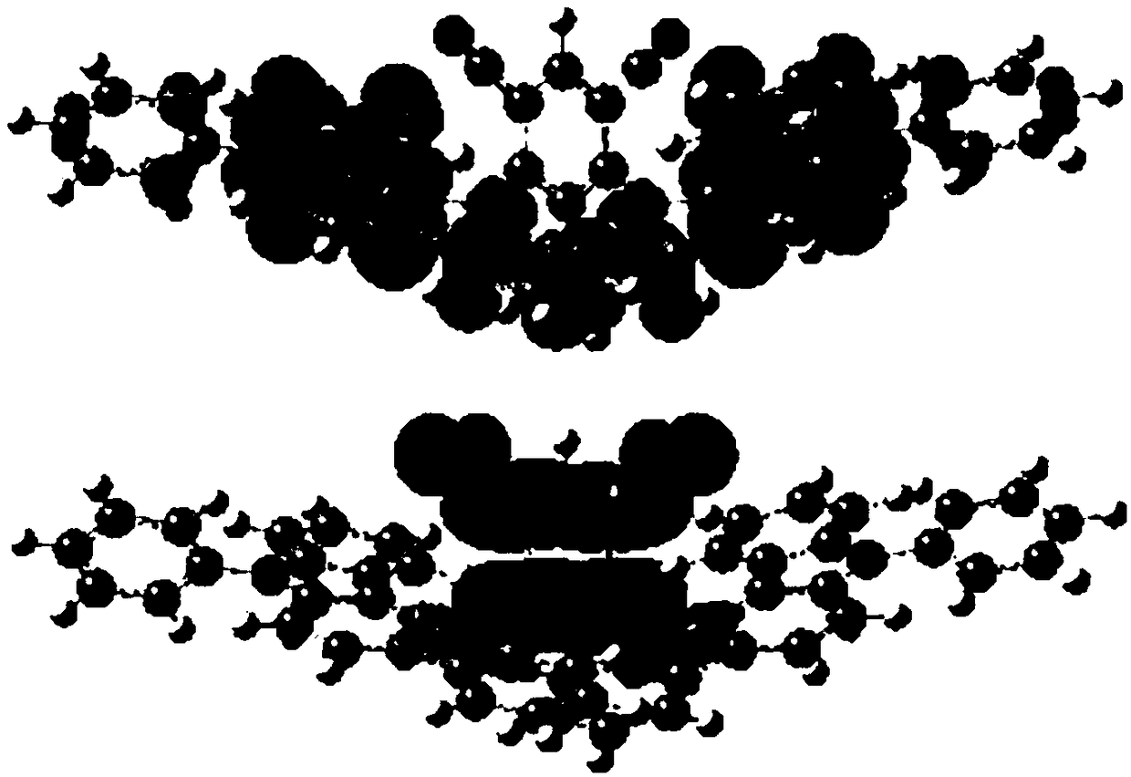
[0058] In one embodiment, the carrier transport material is an electron transport material. For example, the electron transport material is a compound represented by the following general formula:

[0059]

[0060] Preferably, the electron transport material is selected from one or a combination of the following structural formulas:

[0061]

[0062]

[0063]The compounds of the above structural formula are all bipolar materials with stable redox state, and their structure has a certain planarity, and effective π-π stacking can be formed in the crystal structure, which is beneficial to charge transfer and more conducive to electron transport. It has higher electron mobility and better stability than currently used electron transport materials.

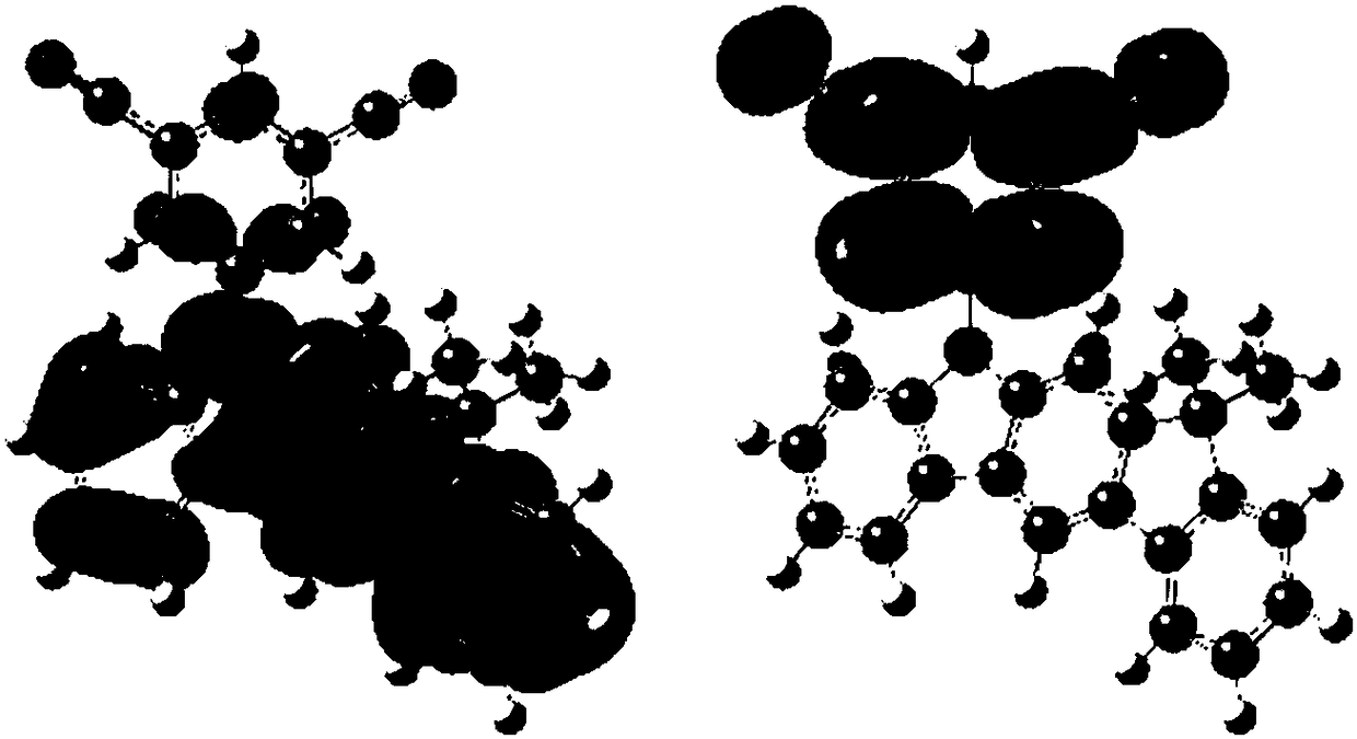
[0064] In another embodiment, the carrier transport material is a hole transport material. For example, the hole transport material is a compound represented by the following general formula:

[0065]

[0066] Preferably...

Embodiment 1

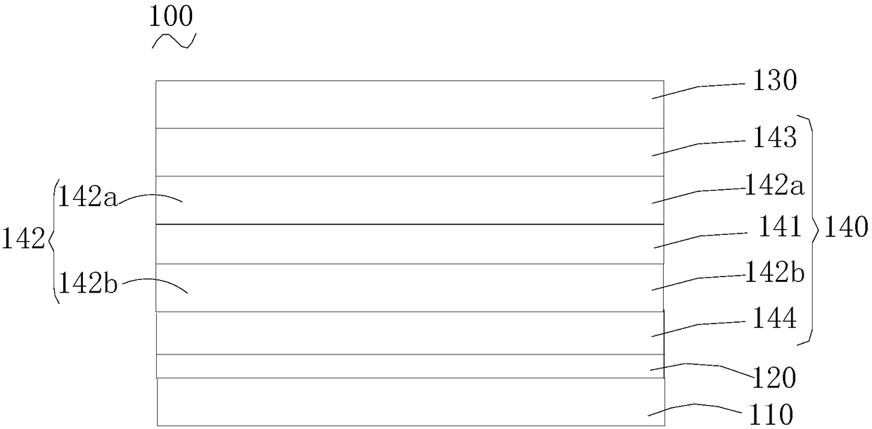
[0098] In this embodiment, the organic host material is selected from the carrier transport material described in the present invention, that is, the host material of the organic light-emitting layer in Example 1 is the same as the hole transport material in the carrier transport material, both of which are of the compound formula 3-12.

[0099] The specific structure of the organic light-emitting device is as follows: ITO (150nm) / HATCN (20nm) / Formula 3-12 (40nm) / Formula 3-12): 3wt%Ir(piq) 2 (acac)(30nm) / TPBi(50nm) / 20%Ag:80%Mg(10nm) / Ag(15nm).

Embodiment 2

[0101] The specific structure of an organic light-emitting device is as follows:

[0102] ITO(150nm) / HATCN(20nm) / Formula 3-12(40nm) / mCBP: 3wt%Ir(piq) 2 (acac)(30nm) / TPBi(50nm) / 20%Ag:80%Mg(10nm) / Ag(15nm).


PUM

PropertyMeasurementUnit
thicknessaaaaaaaaaa
thicknessaaaaaaaaaa

Abstract

The invention relates to a carrier transmission material which is a thermal activation delayed fluorescence material. The thermal activation delayed fluorescence material is selected from compounds formed by matching benzonitrile and carbazole or triphenylamine and compounds formed by matching triazine and carbazole, indole carbazole or triphenylamine. The carrier transmission material, namely thethermal activation delayed fluorescence material (TADF) is small in energy gap among mono-triplet state and high in triplet state, and excitons can be avoided being diffused to a carrier transmissionlayer from an organic light-emitting layer, so that light-emitting efficiency is improved. In addition, the carrier transmission material is high in glass transition temperature Tg and thermostability. Due to bipolarity, electron and hole transmission capacity of the carrier transmission material can be adjusted conveniently by adjusting number and proportion of donor groups and receptor groups.The invention further provides a carrier transmission layer and an organic light-emitting device.

Description

technical field [0001] The invention relates to the technical field of organic light-emitting display, in particular to a carrier transport material, a carrier transport layer and an organic light-emitting device. Background technique [0002] Organic Light Emitting Device (OLED) has become a research hotspot in flat panel display technology due to its advantages of low voltage, low cost, wide viewing angle, fast response, and surface emission. [0003] In an organic light-emitting device, in order to promote better light emission of the organic light-emitting layer, the transport of carriers is generally improved by means of a carrier-transporting material. Carrier transport materials are classified into hole transport materials and electron transport materials. [0004] At present, the hole transport materials in organic light-emitting devices are mainly carbazole compounds and triarylamine compounds, while the electron transport materials are mainly metal chelates and az...

Claims


Application Information

Patent Timeline
Patent Type & Authority Applications(China)
IPC IPC(8): C07D209/86C07D487/04C07C255/58C07D519/00C07D209/94C07D403/04C07D403/14C09K11/06H01L51/54
CPCC09K11/06C07C255/58C07D209/86C07D209/94C07D403/04C07D403/14C07D487/04C07D519/00C09K2211/1029C09K2211/1014C09K2211/1059H10K85/631H10K85/6572
Inventor 段炼宾正杨邱勇赵菲刘嵩
Owner KUNSHAN GO VISIONOX OPTO ELECTRONICS CO LTD
Why Eureka
Try Eureka