Static protection circuit

An electrostatic protection and circuit technology, applied in the direction of circuits, electrical components, electric solid devices, etc., can solve the problems of thin film transistor threshold voltage drift, insulation dielectric breakdown, electrostatic damage, etc., and achieve the effect of improving antistatic ability

Active Publication Date: 2021-03-02
WUHAN CHINA STAR OPTOELECTRONICS TECH CO LTD
View PDF3 Cites 0 Cited by
  • Summary
  • Abstract
  • Description
  • Claims
  • Application Information

AI Technical Summary

Problems solved by technology

When electrostatic discharge occurs, a large current is generated in a short period of time. Once the electrostatic discharge current flows through the semiconductor integrated circuit, it will usually cause electrostatic damage, resulting in the breakdown of the insulating medium, causing the threshold voltage drift of the thin film transistor or gate and source short circuit

Method used


Image

  • Static protection circuit
  • Static protection circuit
  • Static protection circuit

Examples


Embodiment Construction

[0036] In order to further illustrate the technical means adopted by the present invention and its effects, the following describes in detail in conjunction with preferred embodiments of the present invention and accompanying drawings.

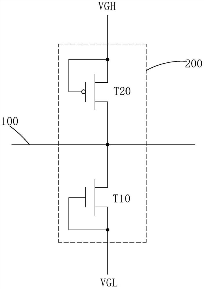
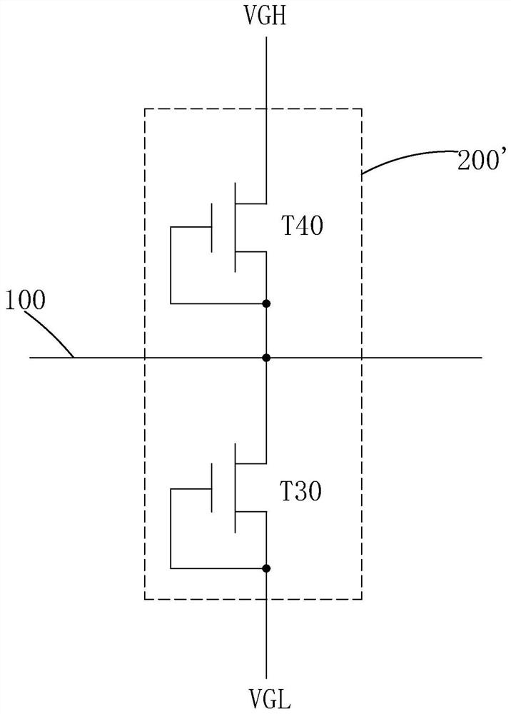
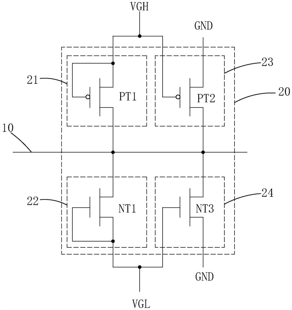
[0037] see image 3 , is the first embodiment of the electrostatic protection circuit of the present invention, the first embodiment of the electrostatic protection circuit of the present invention includes a signal line 10 and an ESD device 20 corresponding to the signal line 10;

[0038] The ESD device 20 includes: a first electrostatic discharge unit 21 electrically connected to the signal line 10 and connected to a constant voltage high potential VGH; a second electrostatic discharge unit 21 electrically connected to the signal line 10 and connected to a constant voltage low potential VGL The unit 22, the third electrostatic discharge unit 23 electrically connected to the signal line 10 and the ground terminal GND and connected to the consta...


PUM


Abstract

The invention provides an electro-static protection circuit. The electro-static protection circuit comprises a signal line and an electro-static discharge (ESD) device, wherein the ESD device is corresponding to the signal line and comprises connection paths and thin film transistors, the connection paths are arranged between the signal line and a constant-voltage high potential, the thin film transistors are arranged on the connection paths between the signal line and the constant-voltage high potential, and in the ESD device, a plurality of connection paths are arranged between the signal line and the constant-voltage high potential and a plurality of thin film transistors are arranged on the connection paths between the signal line and the constant-voltage high potential. By adding an electro-static releasing path or reducing a current generated by electro-static releasing, the anti-static capability of the electro-static protection circuit is effectively improved.

Description

technical field [0001] The invention relates to the field of display technology, in particular to an electrostatic protection circuit. Background technique [0002] During the manufacture and transportation of Thin Film Transistor Liquid Crystal Display (TFT-LCD) and Active-matrix organic light emitting diode (AMOLED) display panels, it is easy to generate electrostatic discharge ( Electro-Static Discharge, ESD) phenomenon. When electrostatic discharge occurs, a large current is generated in a short period of time. Once the electrostatic discharge current flows through the semiconductor integrated circuit, it will usually cause electrostatic damage, resulting in the breakdown of the insulating medium, causing the threshold voltage drift of the thin film transistor or gate and source short circuit. Unless there is a proper discharge path, when the electrostatic charge accumulates to a certain level and is discharged, it will destroy some pixel structures in the display pane...

Claims


Application Information

Patent Timeline
Patent Type & Authority Patents(China)
IPC IPC(8): H01L27/02
CPCH01L27/0266
Inventor 洪光辉
Owner WUHAN CHINA STAR OPTOELECTRONICS TECH CO LTD
Why Eureka
Try Eureka