
A kind of nanocomposite material, preparation method and semiconductor device

A nano-composite material and device technology, applied in the field of quantum dots, can solve the problems that the requirements of nano-composite materials of semiconductor devices cannot be met, and the luminous performance needs to be improved, and achieve the effect of satisfying the comprehensive performance requirements and high luminous efficiency.

Active Publication Date: 2021-05-18
TCL CORPORATION
View PDF12 Cites 0 Cited by
  • Summary
  • Abstract
  • Description
  • Claims
  • Application Information

AI Technical Summary

Problems solved by technology

[0013] In view of the above-mentioned deficiencies in the prior art, the object of the present invention is to provide a nanocomposite material, a preparation method and a semiconductor device, aiming at solving the problem that the luminescent performance of the quantum dot material prepared by the existing preparation method needs to be improved and cannot meet the requirements of the semiconductor device for nanometer Composite Material Requirements Questions

Method used


Image

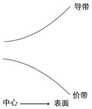
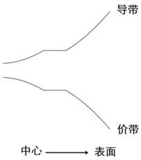
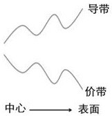
  • A kind of nanocomposite material, preparation method and semiconductor device
  • A kind of nanocomposite material, preparation method and semiconductor device
  • A kind of nanocomposite material, preparation method and semiconductor device

Examples


Embodiment 1

[0114] Example 1: Preparation of quantum dots based on CdZnSeS / CdZnSeS

[0115] First, the precursor of cationic Cd, the precursor of cationic Zn, the precursor of anionic Se and the precursor of anionic S are injected into the reaction system to form Cd y Zn 1-y Se b S 1-b layer (where 0≤y≤1, 0≤b≤1); continue to inject the precursor of cation Cd, the precursor of cation Zn, the precursor of anion Se and the precursor of anion S into the reaction system, in the above Cd y Zn 1-y Se b S 1-b Cd is formed on the surface of the layer z Zn 1-z Se c S 1-c layer (where 0≤z≤1, and z is not equal to y, 0≤c≤1); under certain reaction conditions such as heating temperature and heating time, Cd in the inner and outer nanocrystals (that is, the above two-layer compounds) will interact with each other. The exchange of Zn ions; since the migration distance of cations is limited and the longer the migration distance, the less chance of migration, it will y Zn 1-y Se b S 1-b Laye...

Embodiment 2

[0116] Example 2: Preparation of quantum dots based on CdZnS / CdZnS

[0117] First, the precursor of cationic Cd, the precursor of cationic Zn and the precursor of anion S are injected into the reaction system to form Cd first. y Zn 1-y S layer (where 0≤y≤1); Continue to inject the precursor of cationic Cd, the precursor of cationic Zn and the precursor of anionic S into the reaction system, and the above-mentioned Cd y Zn 1-y Cd is formed on the surface of the S layer z Zn 1-z S layer (where 0≤z≤1, and z is not equal to y); under certain reaction conditions such as heating temperature and heating time, the exchange of Cd and Zn ions in the inner and outer nanocrystals (that is, the above two-layer compounds) occurs. ; Since the migration distance of cations is limited and the longer the migration distance is, the less chance of migration occurs, so it will be in the Cd y Zn 1-y S layer and Cd z Zn 1-z A graded alloy composition distribution of Cd content and Zn content...

Embodiment 3

[0118] Example 3: Preparation based on CdZnSe / CdZnSe quantum dots

[0119] First, the precursor of cationic Cd, the precursor of cationic Zn and the precursor of anionic Se are injected into the reaction system to form Cd first y Zn 1-y Se layer (where 0≤y≤1); Continue to inject the precursor of cationic Cd, the precursor of cationic Zn and the precursor of anionic Se into the reaction system, and the above-mentioned Cd y Zn 1-y Cd is formed on the surface of the Se layer z Zn 1-z Se layer (where 0≤z≤1, and z is not equal to y); under certain reaction conditions such as heating temperature and heating time, the exchange of Cd and Zn ions in the inner and outer nanocrystals occurs; due to the limited migration distance of cations And the farther the migration distance is, the smaller the probability of migration occurs, so it will be in the Cd y Zn 1-y Se layer and Cd z Zn 1-z A graded alloy composition distribution of Cd content and Zn content is formed near the interf...


PUM

PropertyMeasurementUnit
wavelengthaaaaaaaaaa

Abstract

The invention discloses a nanocomposite material, a preparation method and a semiconductor device. The method comprises the steps of: adding one or more cation precursors at predetermined positions in the radial direction; adding one or more cation precursors simultaneously under certain conditions the anion precursor, the cationic precursor reacts with the anion precursor to form a nanocomposite material, and the luminescence peak wavelength of the nanocomposite material appears one or more of blue-shift, red-shift and unchanged during the reaction , so as to achieve the alloy composition distribution at the predetermined position. The nanocomposite material prepared by the above preparation method not only achieves a more efficient luminous efficiency of the nanocomposite material, but also better meets the comprehensive performance requirements of the semiconductor device and the corresponding display technology for the nanocomposite material. Ideal quantum dot luminescent material for display technology.

Description

technical field [0001] The invention relates to the field of quantum dots, in particular to a nanocomposite material, a preparation method and a semiconductor device. Background technique [0002] Quantum dots are special materials that are confined to the nanometer scale in three dimensions. This remarkable quantum confinement effect makes quantum dots have many unique nanometer properties: continuous tunable emission wavelength, narrow emission wavelength, Wide absorption spectrum, high luminescence intensity, long fluorescence lifetime and good biocompatibility. These characteristics make quantum dots have broad application prospects in the fields of flat panel display, solid-state lighting, photovoltaic solar energy, and biomarkers. Especially in the field of flat panel display applications, quantum dot light-emitting diodes (QLEDs) based on quantum dot materials have been used in display image quality, device performance, manufacturing by virtue of the characteristics ...

Claims


Application Information

Patent Timeline
Patent Type & Authority Patents(China)
IPC IPC(8): H01L33/04H01L33/00H01L33/26B82Y40/00
CPCB82Y40/00H01L33/005H01L33/04H01L33/26
Inventor 杨一行刘政钱磊
Owner TCL CORPORATION
Learn More