Thin film and its preparation method and qled device
A technology for thin films and devices, applied in the field of thin films and their preparation, can solve the problem that the luminous efficiency of QLED devices needs to be improved, and achieve the effect of satisfying comprehensive performance requirements and high luminous efficiency
- Summary
- Abstract
- Description
- Claims
- Application Information
AI Technical Summary
Problems solved by technology
Method used
Image
Examples
preparation example Construction
[0077] The present invention also provides a preferred embodiment of a thin film preparation method, which includes the steps of:
[0078] preparing the first dielectric layer;
[0079] preparing a first metal layer on the first dielectric layer;
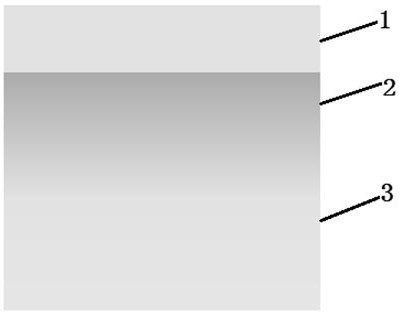
[0080] Coating a blend solution of the second medium and the second metal on the first metal layer, and preparing a graded layer formed by the second metal and the second medium on the first metal layer under heating conditions;
[0081] From a position close to the first metal layer to a direction away from the first metal layer, the mass concentration of the second medium in the graded layer increases from low to high.
[0082] The present invention also provides a preferred embodiment of a thin film preparation method, which includes the steps of:
[0083] Coating a blend solution of the first medium and the first metal on the substrate, and preparing a first graded layer formed by the first metal and the first medium under hea...
Embodiment 1
[0095] The preparation steps of the QLED device are as follows:
[0096] Evaporate a layer of 20nm TiO on the glass ITO substrate x ;
[0097] Then mix 10mg of zinc acetate dihydrate and 2mL of methoxyethanol, heat at 60°C for 30min, add 200μL of ethanolamine, and heat at 60°C for 30min. Add 2 mg of nano-Ag, keep it for 30 minutes without heating, and let it stand for 24 hours to obtain a mixed solution. The mixed solution was spin-coated and heated at 80° C. for 30 min to form a thin film.
[0098] Preparation of QD (20nm), TAPC (40nm), MoO in sequence on the thin film x (4nm) and Ag to obtain a QLED device whose intensity is shown in Figure 4 .
Embodiment 2
[0100] The preparation steps of the QLED device are as follows:
[0101] Prepare a mixed solution: mix 10 mg of zinc acetate dihydrate and 2 mL of methoxyethanol, heat at 60°C for 30 minutes; add 200 μL of ethanolamine, and heat at 60°C for 30 minutes. Add 2mg of nano-Ag, keep it for 30min without heating, and let it stand for 24hr.
[0102] The above mixed solution was spin-coated on a glass ITO substrate, and heated at 80° C. for 3 min. Move it into a vacuum chamber, evacuate to 1000Pa, flush into Ar, and keep it for 30min;
[0103] Then sputter a layer of 20nm TiO to form a thin film.
[0104] QD (20nm), TAPC (40nm), MoOx (4nm) and Ag are sequentially prepared on the film to obtain a QLED device. The intensity of the QLED device is shown in Figure 4 .
PUM
 Abstract
Description
Claims
Application Information


