Overall FPGA automated layout method based on analytical method

A technology of analysis method and layout method, applied in special data processing applications, instruments, electrical digital data processing, etc., can solve problems such as difficult to meet timing constraints, and achieve the effect of optimizing quality and speed

Active Publication Date: 2018-07-17
SHANGHAI FUDAN MICROELECTRONICS GROUP
View PDF2 Cites 15 Cited by
  • Summary
  • Abstract
  • Description
  • Claims
  • Application Information

AI Technical Summary

Problems solved by technology

At present, the scale of FPGA is getting bigger and bigger, and the structure is getting more and more complex. There are more and more types of logic unit modules, and it includes large devices such as DSP (Digital Signal Processor) and RAM (Random Access Memory). Logic units, and the wiring between some units are fixed connections, such as Carry Chain (carry chain) and Shift Register (shift register), etc., which limit the random placement of logic units, especially in timing In terms of constraints, since the layout plays a decisive role in the speed of the FPGA layout, the timing constraints must be taken into account during the layout process, otherwise it is difficult to meet the timing constraints through subsequent optimization such as routing.

Method used


Image

  • Overall FPGA automated layout method based on analytical method
  • Overall FPGA automated layout method based on analytical method
  • Overall FPGA automated layout method based on analytical method

Examples


Embodiment Construction

[0039] Combine the following Figure 1 to Figure 6 , the present invention will be further elaborated by specifying a preferred specific embodiment.

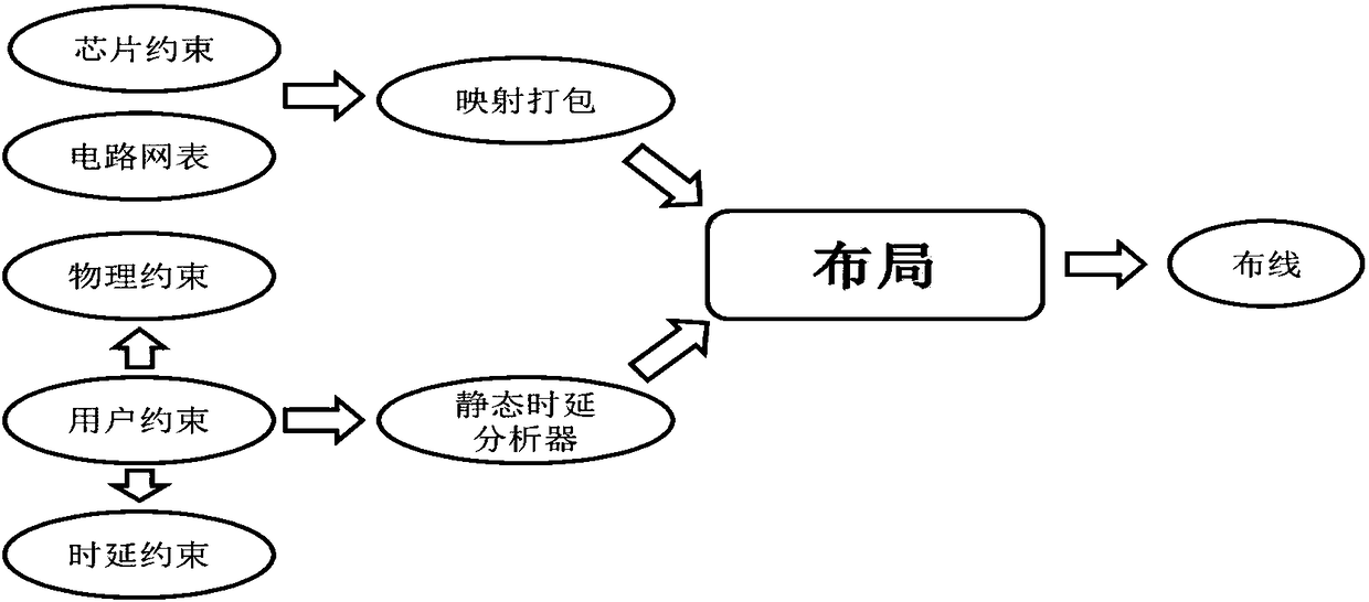
[0040] Such as figure 1 Shown, the design flowchart of the overall FPGA automatic layout method based on the analysis method provided by the present invention comprises the following steps:

[0041] S1. Pack and input FPGA chip constraint information and circuit netlist information through mapping;

[0042] S2. Inputting the user-constrained delay information of the FPGA through a static delay analyzer;

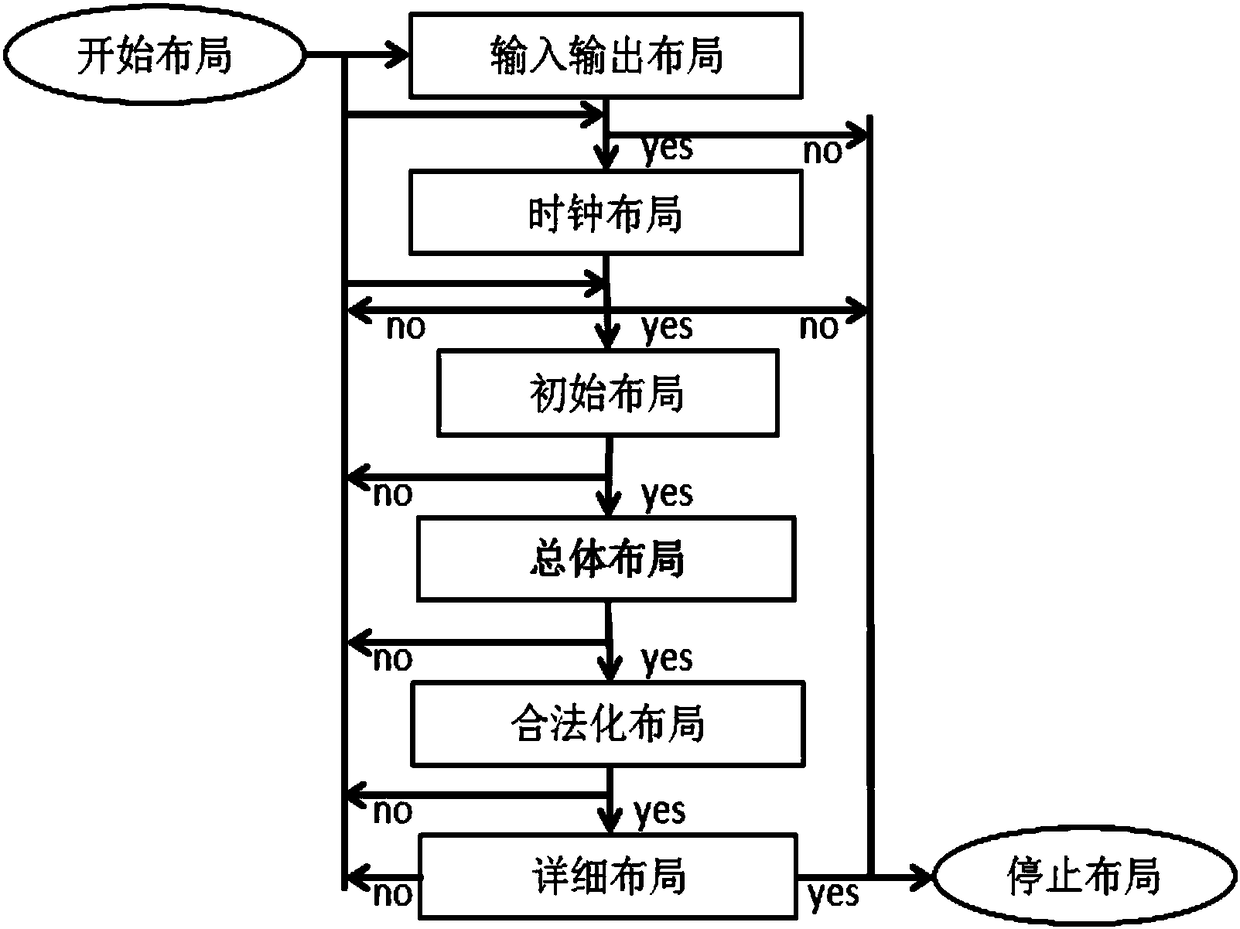
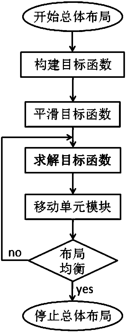
[0043] S3. According to the input chip constraint information, circuit netlist information and user constraint information, each circuit unit module is automatically placed in the corresponding position in the entire chip physical design, specifically including sequential input and output layout, global clock layout, and initial layout. , overall layout, legalized layout and detailed layout;

[0044] S4. Outputting the circ...


PUM


Abstract

Disclosed is an overall FPGA automated layout method based on an analytical method. The layout method comprises the steps that S1, constraint information and circuit netlist information are packed andinput through mapping; S2, time delay information of user constraints is input through a static time delay analyzer; S3, each circuit unit module is automatically laid out in corresponding positionsin a physical design of a chip according to physical constraints designated by a user, and an input and output layout, a global clock layout, an initial layout, an overall layout, a legitimation layout and a detailed layout are involved; according to the overall layout, a conjugate gradient method based on a mixed step-length adjustment strategy is adopted for solving according to the initial positions of the circuit unit modules and circuit topological connection, a step-length calculation manner is dynamically adjusted aiming at the circuit unit modules of different levels and layout states,and the circuit unit modules are distributed; S4, the circuit netlist information is output. By means of the layout method, rapid automated layout is conducted on a chip layout, so that the line length and time delay of a network meet the user constraints; by adjusting a step-length optimization strategy of the overall layout, the quality and speed of the layout are optimized.

Description

technical field [0001] The present invention relates to a kind of FPGA automatic layout method, specifically refers to a kind of overall FPGA automatic layout method based on analytical method, belongs to the field of integrated circuit design, especially belongs to a kind of semi-custom circuit FPGA (Field Programmable Gate) in the field of application specific integrated circuit Array, Field Programmable Gate Array) automatic layout related technical field category. Background technique [0002] FPGA adopts the concept of logic cell array (LCA, Logic Cell Array), and the internal circuit unit modules include: configurable logic module (CLB, Configurable Logic Block), input and output module (IOB, Input Output Block) and internal connection Line (Interconnect) and other parts. The FPGA chip is a two-dimensional structure, each point corresponds to a CLB, and each CLB contains a slice structure SLICE, and the SLICE contains a gate-level table (GATE). FPGA is a programmable...

Claims


Application Information

Patent Timeline
Patent Type & Authority Applications(China)
IPC IPC(8): G06F17/50
CPCG06F30/392
Inventor 王似飞叶翼李小南吴昌
Owner SHANGHAI FUDAN MICROELECTRONICS GROUP
Why Eureka
Try Eureka