Eureka AIR delivers breakthrough ideas for toughest innovation challenges, trusted by R&D personnel around the world.

Organic light-emitting diode and method for making the same, and display device

A technology for light-emitting diodes and a manufacturing method, which is applied to the manufacture of electric solid-state devices, semiconductor devices, and semiconductor/solid-state devices, etc., can solve the problems of affecting the light-emitting characteristics of organic light-emitting diodes, affecting the light-emitting efficiency of organic light-emitting diodes, etc. The effect of improving brightness and increasing light transmittance

Active Publication Date: 2018-07-20
WUHAN CHINA STAR OPTOELECTRONICS SEMICON DISPLAY TECH CO LTD
View PDF3 Cites 3 Cited by
  • Summary
  • Abstract
  • Description
  • Claims
  • Application Information

AI Technical Summary

Problems solved by technology

[0002] Traditional organic light-emitting diodes include an anode, a light-emitting layer and a cathode. The light emitted by an organic light-emitting diode is emitted upward from the cathode. The anode generally adopts the structure of ITO / Ag / ITO (indium tin oxide / silver / indium tin oxide), and Ag is used as The reflective layer can well reflect the light emitted by the organic light-emitting diode upwards, but the transmittance of the top layer ITO near the light-emitting layer is only about 75% when the wavelength of visible light is 550nm, so that part of the light reflected by Ag cannot penetrate the top layer ITO And affect the luminous efficiency of organic light-emitting diodes, thereby seriously affecting the light-emitting characteristics of organic light-emitting diodes

Method used


Image

  • Organic light-emitting diode and method for making the same, and display device
  • Organic light-emitting diode and method for making the same, and display device
  • Organic light-emitting diode and method for making the same, and display device

Examples


Embodiment Construction

[0018] The following will clearly and completely describe the technical solutions in the embodiments of the present application with reference to the drawings in the embodiments of the present application. Obviously, the described embodiments are only some of the embodiments of the present application, not all of them. Based on the embodiments in this application, all other embodiments obtained by persons of ordinary skill in the art without making creative efforts belong to the scope of protection of this application.

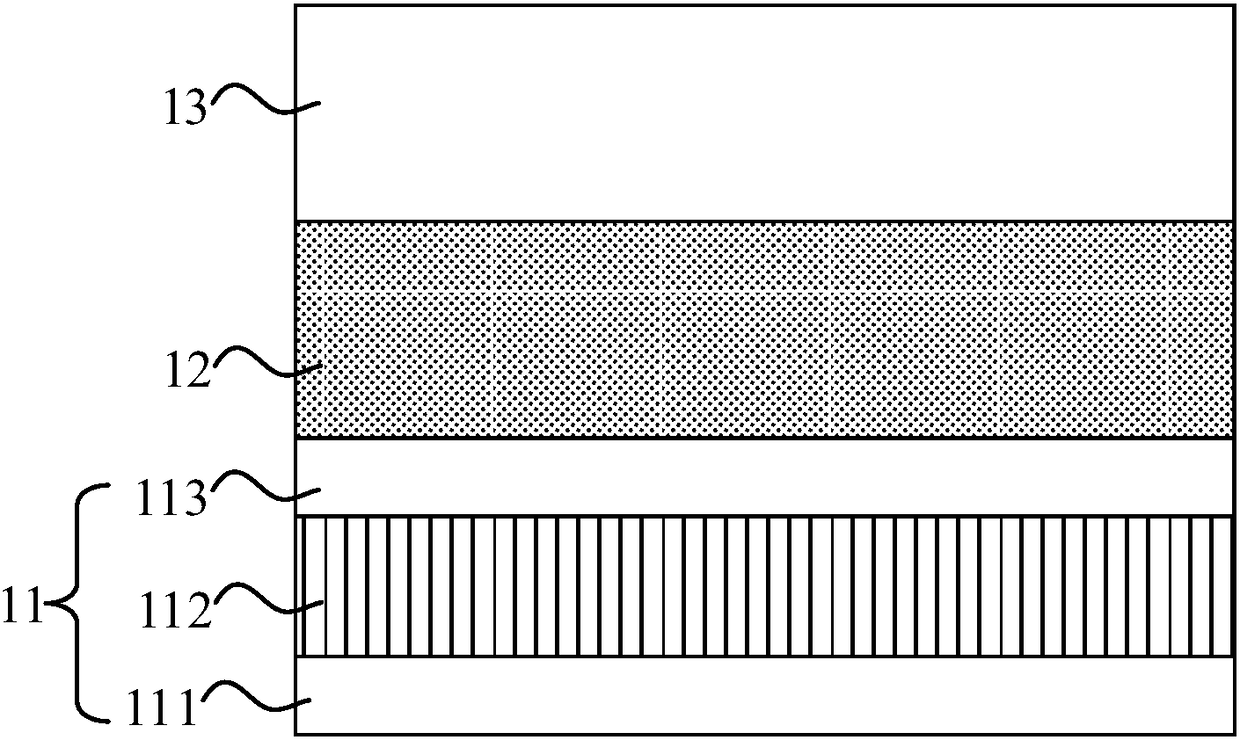
[0019] refer to figure 1 , figure 1 It is a schematic structural diagram of an embodiment of an organic light emitting diode provided in this application, and the organic light emitting diode includes:

[0020] The first electrode 11 , the light emitting layer 12 and the second electrode 13 are stacked.

[0021] The first electrode 11 includes a lower electrode layer 111 , a reflective layer 112 and an upper electrode layer 113 which are stacked. The upper e...


PUM


Abstract

The application discloses an organic light-emitting diode and a method for making the same, and a display device. The organic light-emitting diode comprises a first electrode, a light emitting layer and a second electrode that are laminated. The first electrode consists of a lower electrode layer, a reflective layer and an upper electrode layer that are laminated; and the upper electrode layer isadjacent to the light emitting layer. The upper electrode is a transparent electrode; and a difference value between a maximum size and a minimum size of the crystal grain included by the upper electrode is less than or equal to 0.05 microns and the crystal grain are distributed uniformly. Therefore, the luminous efficiency of the organic light emitting diode is enhanced and the brightness of theorganic light-emitting diode is improved.

Description

technical field [0001] The present application relates to the field of display technology, in particular to an organic light emitting diode, a manufacturing method thereof, and a display. Background technique [0002] Traditional organic light-emitting diodes include an anode, a light-emitting layer and a cathode. The light emitted by an organic light-emitting diode is emitted upward from the cathode. The anode generally adopts the structure of ITO / Ag / ITO (indium tin oxide / silver / indium tin oxide), and Ag is used as The reflective layer can well reflect the light emitted by the organic light-emitting diode upwards, but the transmittance of the top layer ITO near the light-emitting layer is only about 75% when the wavelength of visible light is 550nm, so that part of the light reflected by Ag cannot penetrate the top layer ITO The luminous efficiency of the organic light emitting diode is affected, thereby seriously affecting the light emitting characteristics of the organic ...

Claims


Application Information

Patent Timeline
Patent Type & Authority Applications(China)
IPC IPC(8): H01L51/52H01L51/56H01L27/32
CPCH10K59/12H10K50/81H10K71/00
Inventor 喻蕾李松杉
Owner WUHAN CHINA STAR OPTOELECTRONICS SEMICON DISPLAY TECH CO LTD
Why Eureka
Eureka Blog
Learn More