OLED anode and manufacturing method thereof, manufacturing method of OLED substrate

A manufacturing method and anode technology, which are used in semiconductor/solid-state device manufacturing, organic semiconductor devices, semiconductor devices, etc., can solve the problems of poor uniformity, uneven arrangement of crystal grains, and unsatisfactory reflectivity, and reduce uniformity. , The effect of improving luminous efficiency and improving reflectivity

Active Publication Date: 2020-07-31
WUHAN CHINA STAR OPTOELECTRONICS SEMICON DISPLAY TECH CO LTD
View PDF6 Cites 0 Cited by
  • Summary
  • Abstract
  • Description
  • Claims
  • Application Information

AI Technical Summary

Problems solved by technology

However, in the current process of using silver to form the reflective layer, such as figure 1 As shown, the uniformity (uniformity) of the crystal grains 11 formed by deposition is relatively poor, generally about 30%, the crystal grains 11 are arranged irregularly, and the reflectivity to light is not ideal, for example, the reflectivity when the wavelength of visible light is 550nm It is only about 97%, which will undoubtedly affect the luminous efficiency of the OLED panel

Method used


Image

  • OLED anode and manufacturing method thereof, manufacturing method of OLED substrate
  • OLED anode and manufacturing method thereof, manufacturing method of OLED substrate
  • OLED anode and manufacturing method thereof, manufacturing method of OLED substrate

Examples


Embodiment Construction

[0026] The following will clearly and completely describe the technical solutions of each exemplary embodiment provided by the present invention with reference to the accompanying drawings in the embodiments of the present invention. In the case of no conflict, the following embodiments and features in the embodiments can be combined with each other. Moreover, the directional terms used throughout the present invention, such as "upper" and "lower", are for better describing the technical solutions of various embodiments, and are not used to limit the protection scope of the present invention.

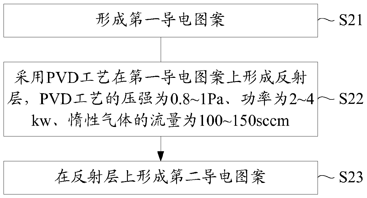
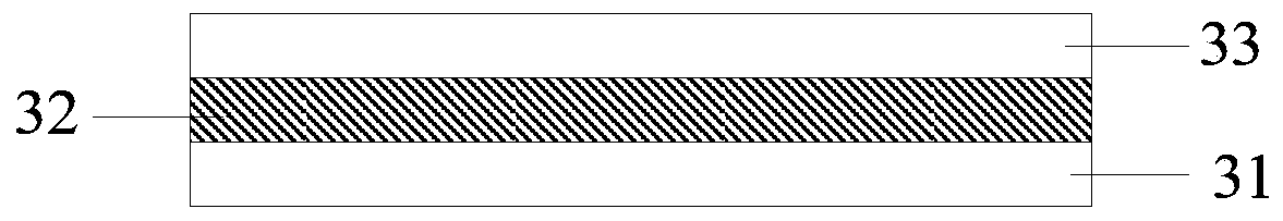
[0027] figure 2 is a schematic flow chart of a method for manufacturing an OLED anode according to an embodiment of the present invention, image 3 It is a structural schematic diagram of an OLED anode according to an embodiment of the present invention. see figure 2 and image 3 , the manufacturing method of the OLED anode includes steps S21-S23.

[0028] S21: forming a first co...


PUM

PropertyMeasurementUnit
reflectanceaaaaaaaaaa

Abstract

The invention discloses an OLED anode, a manufacturing method thereof, and a manufacturing method of an OLED substrate. The manufacturing method of the OLED anode includes: forming a first conductive pattern; forming a reflective layer on the first conductive pattern by using a physical vapor deposition PVD process, the pressure of the PVD process is 0.8-1Pa, the power is 2-4kw, and the inert gas The flow rate is 100-150 sccm; a second conductive pattern is formed on the reflective layer. Based on this, the present invention can reduce the uniformity of crystal grain size in the reflective layer, increase the reflectivity of the reflective layer to visible light, and improve the luminous efficiency of the OLED panel.

Description

technical field [0001] The present invention relates to the display field, in particular to an OLED (Organic Light-Emitting Diode, Organic Light-Emitting Diode) anode, a manufacturing method thereof, and a manufacturing method of an OLED substrate. Background technique [0002] Compared with traditional liquid crystal display panels, OLED panels have advantages such as fast response speed, high contrast ratio, and wide viewing angle, and are regarded as the next-generation display technology. The light-emitting principle of the OLED panel is: apply a voltage to the anode and the cathode, and under the drive of the voltage, electron holes are respectively injected from the cathode and the anode into the electron and hole transport layers, migrate to the light-emitting layer, and meet in the light-emitting layer to form excitons and excite light-emitting molecules to emit visible light. [0003] In the structural design of a top emission (Top emission) OLED panel, silver (Ag)...

Claims


Application Information

Patent Timeline
Patent Type & Authority Patents(China)
IPC IPC(8): H01L51/56H01L51/52H01L27/32
CPCH10K59/12H10K50/81H10K2102/3026H10K59/1201H10K71/00
Inventor 喻蕾李松杉
Owner WUHAN CHINA STAR OPTOELECTRONICS SEMICON DISPLAY TECH CO LTD
Why Eureka
Try Eureka