Image sensor and forming method thereof

An image sensor and patterning technology, applied in the direction of electric solid-state devices, semiconductor devices, electrical components, etc., can solve the problems of less light absorption, difficulty in generating photoelectrons, and low sensitivity

Inactive Publication Date: 2018-07-24
HUAIAN IMAGING DEVICE MFGR CORP
View PDF5 Cites 6 Cited by
  • Summary
  • Abstract
  • Description
  • Claims
  • Application Information

AI Technical Summary

Problems solved by technology

[0004] However, existing infrared image sensors have low sensitivity
Specifically, since the depth of the photodiode is usually small, and the wavelength of infrared rays is usually long (0.76um to 1000um), resulting in too little light absorption during the process of infrared rays passing through the photodiode, it is difficult to generate enough photoelectrons, resulting in reduced sensitivity

Method used


Image

  • Image sensor and forming method thereof
  • Image sensor and forming method thereof
  • Image sensor and forming method thereof

Examples


Embodiment Construction

[0026] In the prior art, infrared image sensors have been widely used in monitoring, automobile, medical and other fields, however, the existing infrared image sensors have low sensitivity.

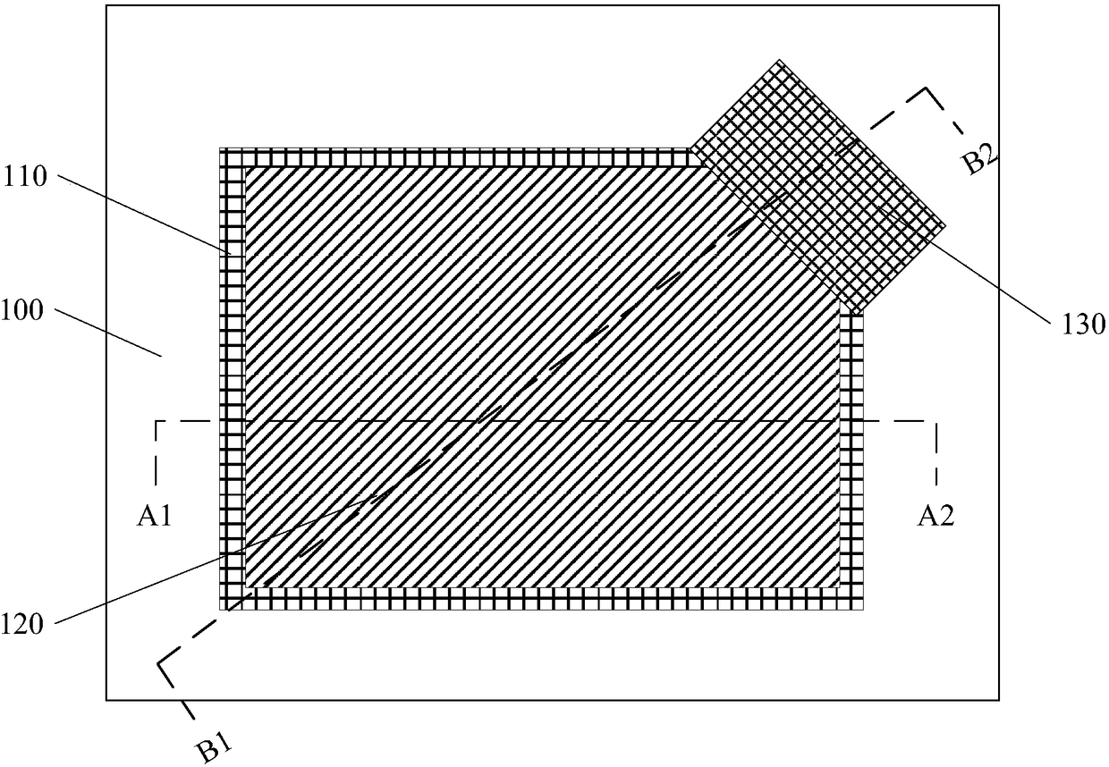
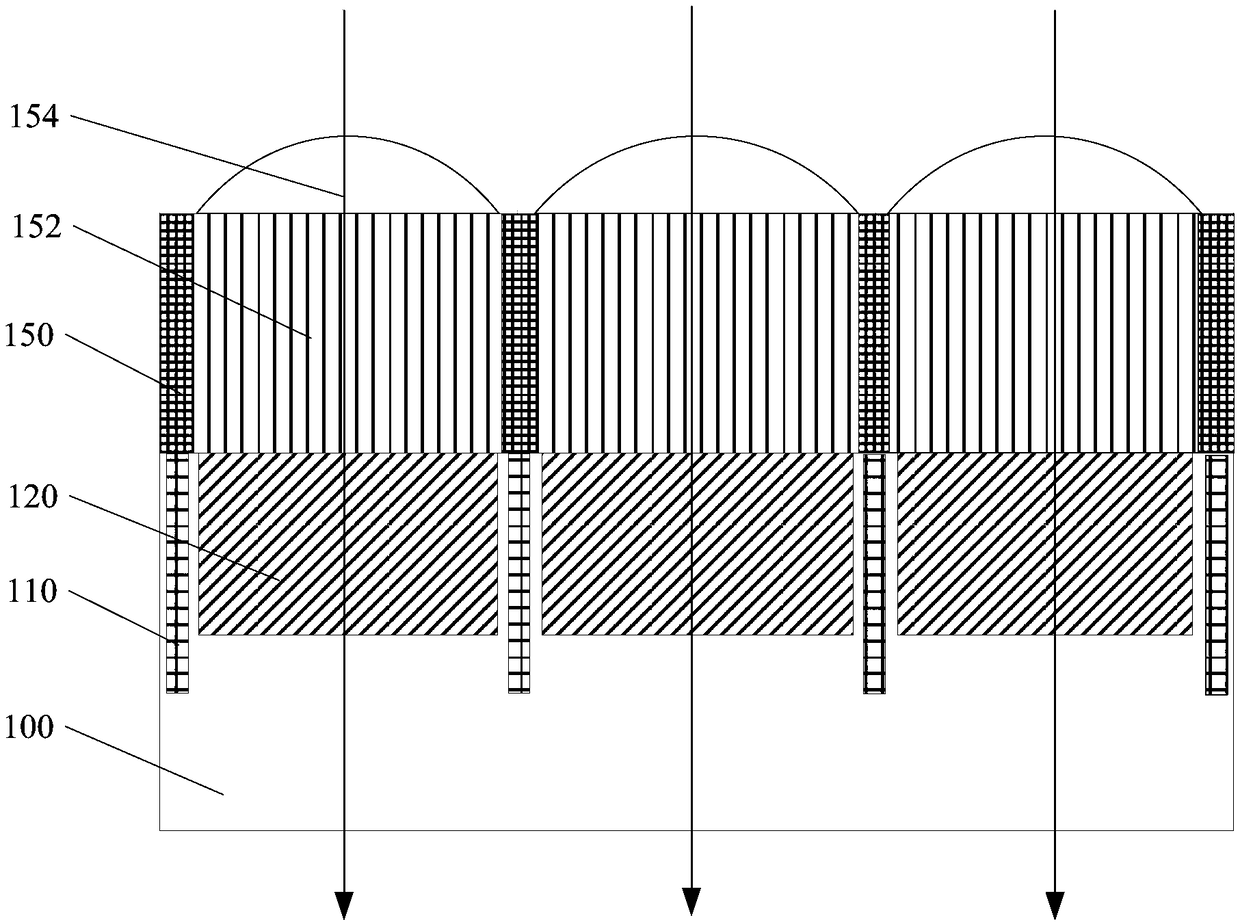
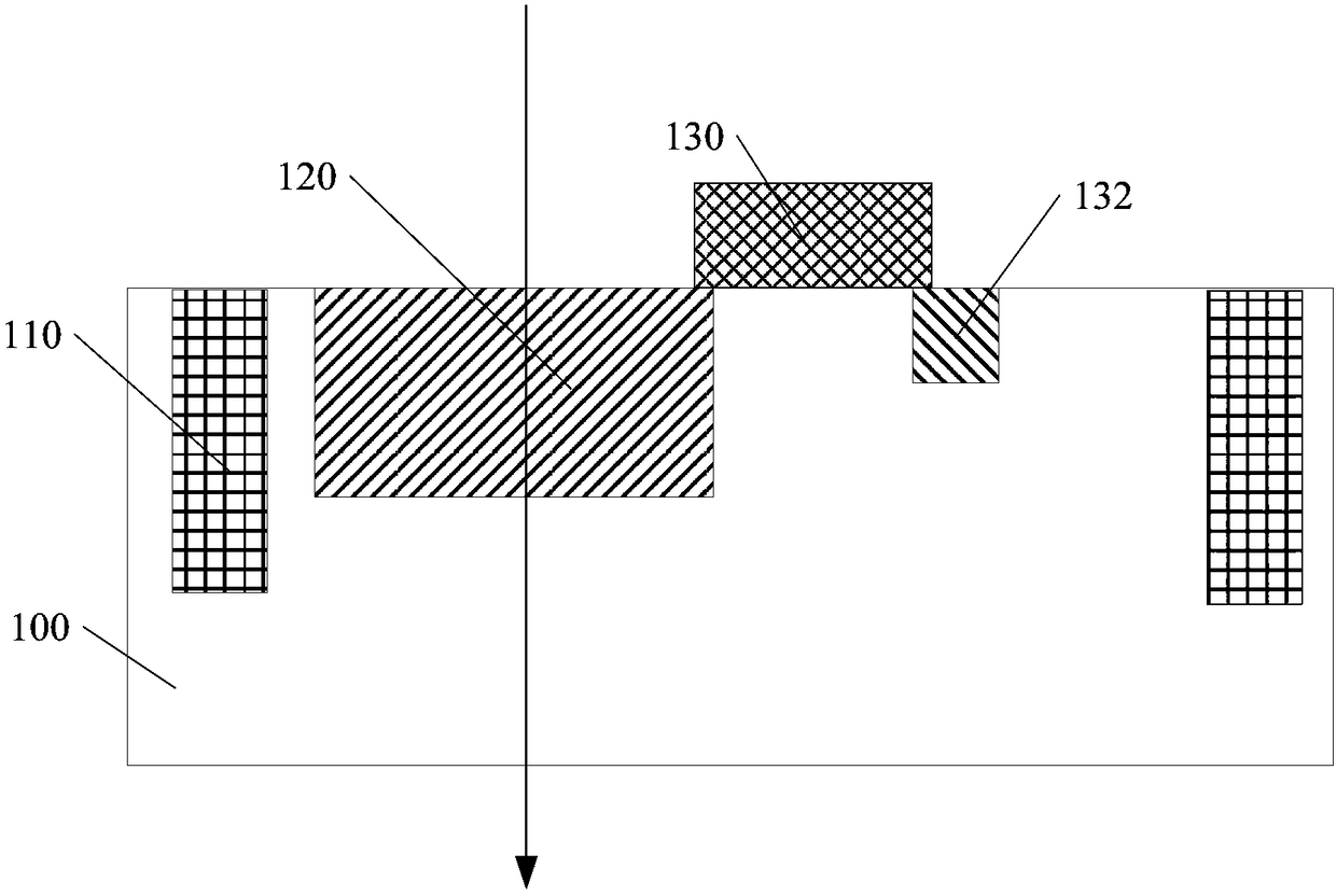
[0027] combined reference Figure 1 to Figure 3 , figure 1 is a top view of an image sensor in the prior art, figure 2 Yes figure 1 Schematic diagram of the cross-sectional structure along the cutting line A1-A2, image 3 Yes figure 1 Schematic diagram of the cross-sectional structure along the cutting line B1-B2.

[0028] The image sensor may include a semiconductor substrate 100 , an isolation structure 110 , a photodiode doped region 120 , a transfer gate 130 and a floating diffusion region 132 .

[0029] Wherein, the isolation structure 110 is located in the semiconductor substrate 100 for isolating adjacent photodiode doped regions 120 .

[0030] The photodiode doped region 120 is located in the semiconductor substrate 100 .

[0031] The transfer gate (Transfer Gate, TG) 130 ...


PUM


Abstract

An image sensor and a forming method thereof are provided. The forming method comprises: providing a semiconductor substrate having a front surface and a back surface; performing first ion implantation on the semiconductor substrate from the front surface of the semiconductor substrate to form a front photodiode doped region; performing second ion implantation on the semiconductor substrate from the back surface of the semiconductor substrate to form a back photodiode doped region, wherein the front photodiode doped region and the back photodiode doped regions communicate with each other. Theforming method can improve the sensitivity of the image sensor.

Description

technical field [0001] The invention relates to the technical field of semiconductor manufacturing, in particular to an image sensor and a forming method thereof. Background technique [0002] Image sensors (Image Sensors) are the core components of camera equipment, which realize the image capture function by converting optical signals into electrical signals. Since the CMOS image sensor (CMOS Image Sensor, CIS) has the advantages of low power consumption and high signal-to-noise ratio, it has been widely used in various fields. [0003] Taking the infrared (Infrared Rays, IR) image sensor as an example, the incident light can be captured by the lens (Micro-lens), and the incident light can be filtered by an IR filter (Colour filter) or other devices to remove irrelevant light, and then use Infrared photons reach the photodiode area and are absorbed by it, forming photoelectrons. [0004] However, existing infrared image sensors have low sensitivity. Specifically, becaus...

Claims


Application Information

Patent Timeline
Patent Type & Authority Applications(China)
IPC IPC(8): H01L27/146
CPCH01L27/14649H01L27/14683
Inventor 内藤逹也黄晓橹
Owner HUAIAN IMAGING DEVICE MFGR CORP
Why Eureka
Try Eureka