Exposure device, exposure device control method, and device manufacturing method
An exposure device and control system technology, which is applied in the field of component manufacturing, can solve problems such as difficult masking, difficult correction of nonlinear control errors, and poor controllability
- Summary
- Abstract
- Description
- Claims
- Application Information
AI Technical Summary
Problems solved by technology
Method used
Image

Examples
Embodiment Construction
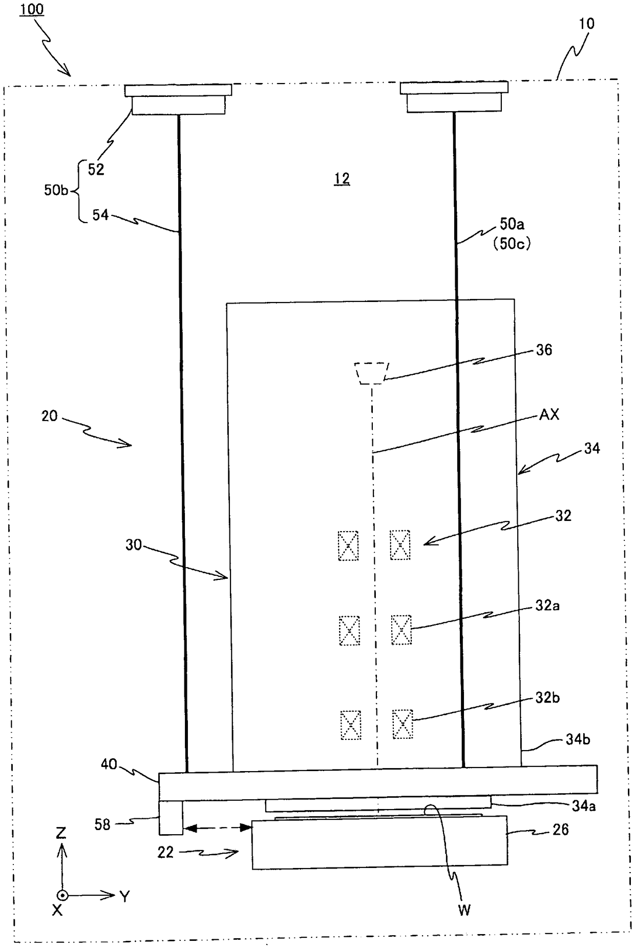
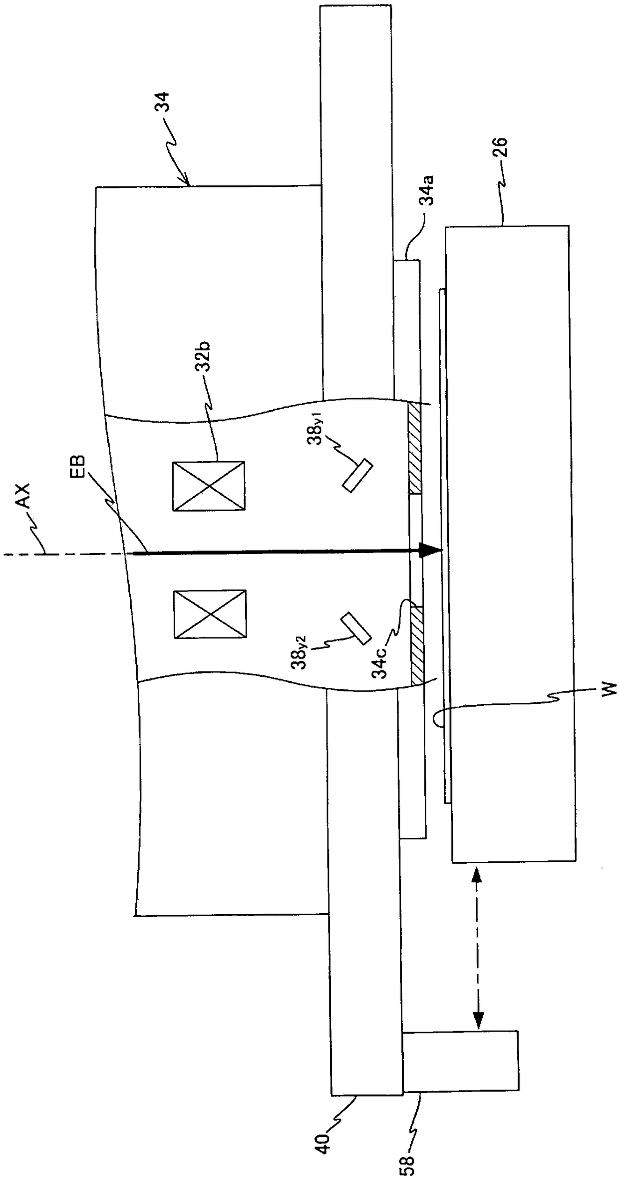
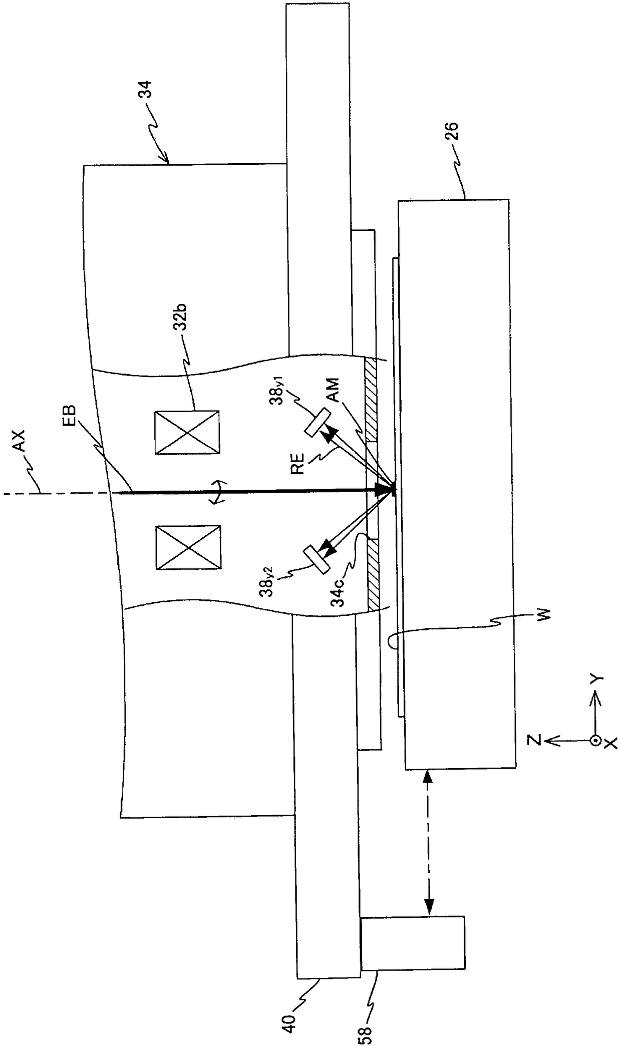
[0026] Below, based on Figure 1 to Figure 11 (B) One embodiment will be described. figure 1 , schematically shows the configuration of an electron beam exposure apparatus 100 according to an embodiment. The electron beam exposure apparatus 100 is equipped with an electron beam optical system as described later, therefore, hereinafter, the Z axis is taken to be parallel to the optical axis of the electron beam optical system, and it moves when performing scanning exposure described later in a plane perpendicular to the Z axis. The scanning direction of the wafer W (stage 26) is defined as the Y-axis direction, the direction perpendicular to the Z-axis and the Y-axis is defined as the X-axis direction, and the rotation (tilt) directions around the X-axis, Y-axis, and Z-axis are respectively The description will be made assuming that the θx, θy, and θz directions are used.
[0027] In this embodiment, a configuration using an electron beam will be described as an example of a ...
PUM
 Abstract
Description
Claims
Application Information
 - R&D
- Intellectual Property
- Life Sciences
- Materials
- Tech Scout
- Unparalleled Data Quality
- Higher Quality Content
- 60% Fewer Hallucinations
Browse by: Latest US Patents, China's latest patents, Technical Efficacy Thesaurus, Application Domain, Technology Topic, Popular Technical Reports.
© 2025 PatSnap. All rights reserved.Legal|Privacy policy|Modern Slavery Act Transparency Statement|Sitemap|About US| Contact US: help@patsnap.com