Photosensitive assembly and preparation method, array substrate and display device thereof

A technology of photosensitive components and array substrates, which is applied in radiation control devices, semiconductor/solid-state device manufacturing, electrical components, etc., and can solve the problems of thin film transistors 11, such as adverse effects on electrical performance and long time

Pending Publication Date: 2018-08-07
BOE TECH GRP CO LTD
View PDF8 Cites 17 Cited by
  • Summary
  • Abstract
  • Description
  • Claims
  • Application Information

AI Technical Summary

Problems solved by technology

[0005] However, because the material of the photosensitive sensing layer 122 usually includes a-Si and other materials containing more hydrogen (H) elements, and the time to form the photosensitive sensing layer 122 is relatively long, therefore, in the process of forming the photosensitive sensing layer 122 In , the H element is easy to diffuse into the channel region (when the thin film transistor is working, the region between the source and the drain in the active layer is the channel region), thus causing adverse effects on the electrical performance of the thin film transistor 11, for example , due to too much H element in the channel region, the thin film transistor 11 is uncontrolled and always in the open state

Method used


Image

  • Photosensitive assembly and preparation method, array substrate and display device thereof
  • Photosensitive assembly and preparation method, array substrate and display device thereof
  • Photosensitive assembly and preparation method, array substrate and display device thereof

Examples


Embodiment Construction

[0031] The following will clearly and completely describe the technical solutions in the embodiments of the present invention with reference to the accompanying drawings in the embodiments of the present invention. Obviously, the described embodiments are only some, not all, embodiments of the present invention. Based on the embodiments of the present invention, all other embodiments obtained by persons of ordinary skill in the art without making creative efforts belong to the protection scope of the present invention.

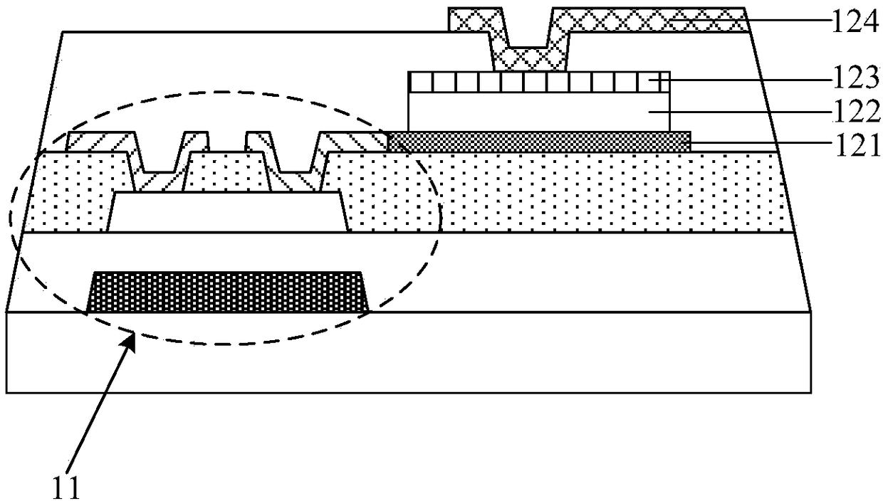
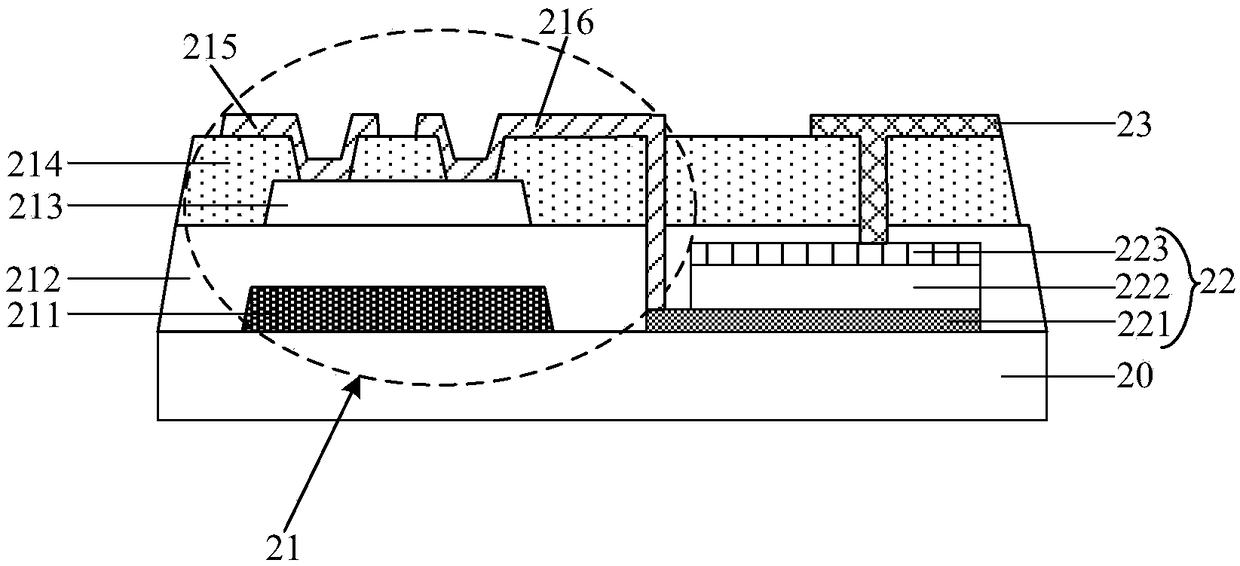
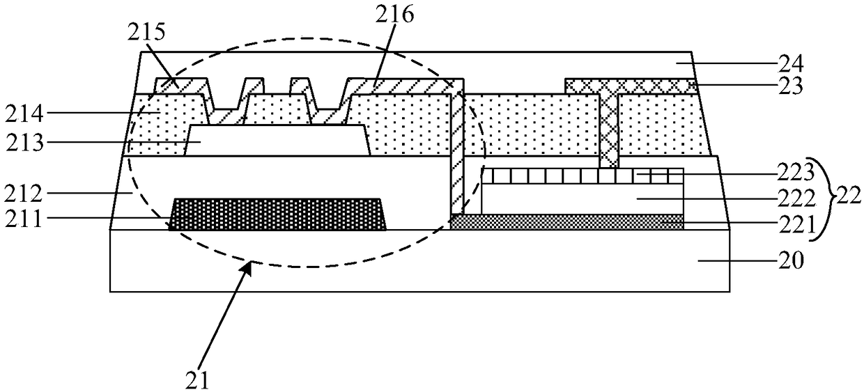
[0032] An embodiment of the present invention provides a photosensitive component, such as figure 2 As shown, it includes a substrate 20, and also includes a thin film transistor 21 and a photosensitive unit 22 arranged in a staggered direction perpendicular to the thickness of the substrate 20, and an insulating layer arranged between the active layer 213 of the thin film transistor 21 and the photosensitive unit 22; The photosensitive unit 22 includes a fir...


PUM


Abstract

The embodiment of the invention provides a photosensitive assembly and a preparation method, an array substrate and a display device thereof, and relates to the technical field of display. The photosensitive assembly can avoid the adverse effect to the electrochemical property of a thin film transistor by H (hydrogen) element in a photosensitive sensing unit. The photosensitive assembly comprisesa substrate, the thin film transistor, a photosensitive unit and an insulation layer, wherein the thin film transistor and the photosensitive unit are staggered along the direction vertical to the thickness direction of the substrate; the insulation layer is arranged between an active layer of the thin film transistor and the photosensitive unit; the photosensitive unit sequentially comprises a first electrode, the photosensitive sensing unit and a second electrode which are sequentially arranged on the substrate; a drain of the thin film transistor is electrically connected with the first electrode; the active layer of the thin film transistor is positioned at one side, away from the substrate, of the insulation layer; the photosensitive unit is positioned at one side, near the substrate,of the insulation layer.

Description

technical field [0001] The invention relates to the field of display technology, in particular to a photosensitive component, a preparation method thereof, an array substrate, and a display device. Background technique [0002] In recent years, organic light emitting diodes (OLEDs) have been widely used in the field of high-performance displays due to their advantages such as self-illumination, wide viewing angle, short response, high luminous efficiency, wide color gamut, and low power consumption. [0003] However, due to the threshold voltage (Vth) drift in the OLED pixel circuit, it is difficult for the existing thin film transistor (Thin Film Transistor, TFT for short) to meet the electrical performance requirements of the OLED display panel. Therefore, compensation technology is required to improve the display quality. [0004] like figure 1 As shown, the prior art is to form the thin film transistor 11 first, and then sequentially form the lower electrode 121 of the ...

Claims


Application Information

Patent Timeline
Patent Type & Authority Applications(China)
IPC IPC(8): H01L27/144H01L27/12H01L27/32H01L21/77
CPCH01L27/1288H01L27/1443H01L27/1446H10K59/60H10K59/12H10K59/123H10K59/1213H10K59/13H01L27/14616H01L27/14643H01L27/14689H01L29/7869H10K59/65
Inventor 刘威
Owner BOE TECH GRP CO LTD
Why Eureka
Try Eureka