Superstructure LED chip and preparation method thereof

A technology of LED chips and superstructures, applied in electrical components, circuits, semiconductor devices, etc., can solve the problems of short service life of vertical LED chips, poor contact between electrodes and substrates, and the bonding surface is not flat enough to improve the effective bonding. performance, shorten the production cycle, and protect from damage

Active Publication Date: 2018-08-10
HEYUAN CHOICORE PHOTOELECTRIC TECH CO LTD
View PDF6 Cites 6 Cited by
  • Summary
  • Abstract
  • Description
  • Claims
  • Application Information

AI Technical Summary

Problems solved by technology

[0004] In order to overcome the deficiencies in the prior art, one of the purposes of the present invention is to provide a superstructure LED chip to overcome the problems of the traditional vertical LED chip, such as the bonding failure caused by the unevenness of the bonding surface and the limited bonding force. Poor contact with the substrate, short service life of the vertical LED chip, etc.

Method used


Image

  • Superstructure LED chip and preparation method thereof
  • Superstructure LED chip and preparation method thereof
  • Superstructure LED chip and preparation method thereof

Examples


Embodiment 31

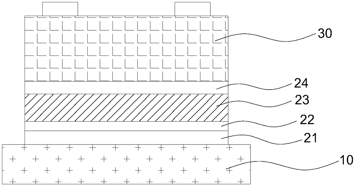
[0050] Step 1: A 300nm-thick AlN buffer layer, a 700nm-thick non-doped GaN layer, a 2000nm-thick n-type GaN layer, a 120nm-thick multi-quantum well light-emitting layer and 200nm thick p-type GaN layer.

[0051] Step 2: On the p-type GaN layer, a 100nm-thick Ni / Ag / Ni / Ag reflective layer and a 20nm-thick Ti protective layer are sequentially deposited using electron beam evaporation equipment.

[0052] Step 3: Using ICP etching technology, form a through-hole structure on the Ti protective layer through the Ti protective layer, reflective layer, p-type GaN layer, multi-quantum well light-emitting layer and part of the n-type GaN layer. The bottom of the through-hole structure is located at within the n-type GaN layer.

[0053] Step 4: Deposit SiO with a thickness of 10 μm on the Ti protective layer and in the via structure by PECVD 2 Insulation.

[0054] Step 5: Removal of SiO at the bottom of the via structure using selective acid etching 2 The insulating layer, the insulat...

Embodiment 32

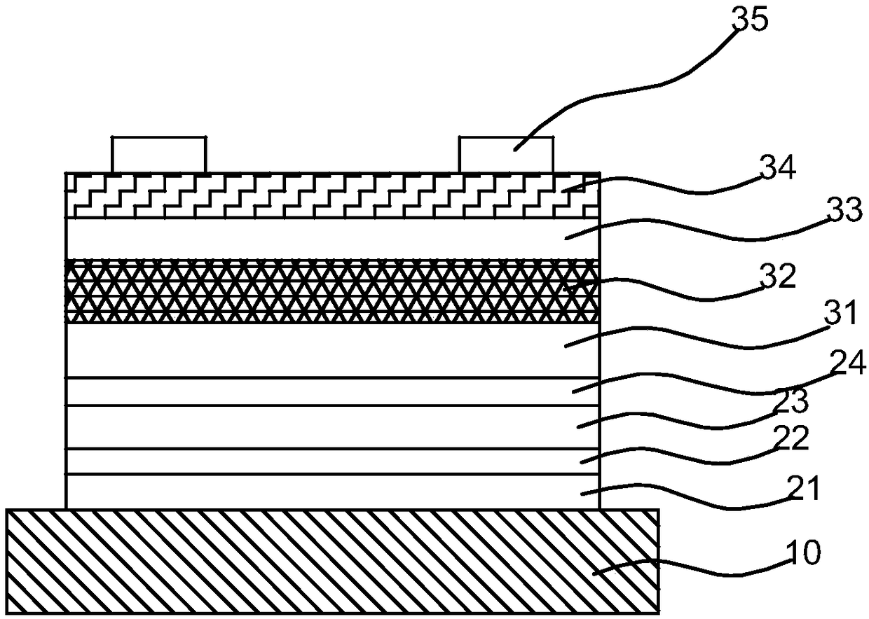
[0064]Step 1: Grow a 1200nm-thick non-doped GaN layer, a 2500nm-thick n-type GaN layer, a 150nm-thick multi-quantum well light-emitting layer and a 200nm-thick p-type GaN layer on the surface of the sapphire substrate sequentially by metal-organic compound vapor deposition technology .

[0065] Step 2: A 400nm thick Ni / Ag / Ni / Ag reflective layer and a 100nm thick Ti protective layer are sequentially deposited on the p-type GaN layer using thermal evaporation equipment.

[0066] Step 3: Using ICP etching technology, form a through-hole structure on the Ti protective layer through the Ti protective layer, reflective layer, p-type GaN layer, multi-quantum well light-emitting layer and part of the n-type GaN layer. The bottom of the through-hole structure is located at within the n-type GaN layer.

[0067] Step 4: Deposit SiN with a thickness of 10 μm on the Ti protective layer and in the via structure by PECVD 1.8 Insulation.

[0068] Step 5: Removal of SiN at the bottom of the...


PUM


Abstract

The invention discloses a superstructure LED chip, comprising a bonded substrate and a light emitting hierarchical structure; a first adhesion layer, a barrier layer, a bonded layer and a second adhesion layer are arranged between the bonded substrate and the light emitting hierarchical structure in sequence; the first adhesion layer is adhered to the bonded substrate; the second adhesion layer isadhered to the light emitting hierarchical structure, wherein the first adhesion layer is a Cr adhesion layer, Pt adhesion layer or a Cr/Pt adhesion layer; the barrier layer is a Ti barrier layer; the bonded layer is formed by multiple Ni/Sn bonded layers in a stacked manner; in the Ni/Sn bonded layers, the thickness of the Sn layer is 1-8 times of that of the Ni layer; and the second adhesion layer is a Ti adhesion layer. The invention also discloses a preparation method of the superstructure LED chip. According to the superstructure LED chip disclosed in the invention, the bonded substrateand the light emitting hierarchical structure are high in bonding, so that an electrode and the substrate are high in contact, and long service life can be achieved.

Description

technical field [0001] The invention relates to the technical field of semiconductors, in particular to the technical field of superstructure LED chips, in particular to a superstructure LED chip and a preparation method of the superstructure LED chip. Background technique [0002] Light Emitting Diode (LED for short) has the characteristics of energy saving, environmental protection, long life, and small size, and has been widely used in many fields such as indoor lighting, display, and traffic indication. In recent years, vertical LED chips have become the mainstream trend of LED technology because they overcome the technical bottlenecks of traditional horizontal structures in terms of efficiency, heat dissipation, and reliability. [0003] A vertical LED chip usually includes a substrate (base) and a light-emitting hierarchical structure on the substrate. The light-emitting hierarchical structure includes a P-N junction composed of an n-type GaN layer, a multi-quantum wel...

Claims


Application Information

Patent Timeline
Patent Type & Authority Applications(China)
IPC IPC(8): H01L33/62H01L33/00
CPCH01L33/0075H01L33/0093H01L33/62
Inventor 李国强
Owner HEYUAN CHOICORE PHOTOELECTRIC TECH CO LTD
Why Eureka
Try Eureka