An electroluminescence display panel, its preparation method and display device

An electroluminescent display and panel technology, which is applied to circuits, electrical components, electrical solid devices, etc., can solve problems such as coffee ring effect, and achieve the effect of improving the uniformity of film thickness and improving the display effect.

Active Publication Date: 2019-10-01
BOE TECH GRP CO LTD +1
View PDF4 Cites 0 Cited by
  • Summary
  • Abstract
  • Description
  • Claims
  • Application Information

AI Technical Summary

Problems solved by technology

[0004] Embodiments of the present invention provide an electroluminescence display panel, its preparation method, and a display device to solve the problem of the coffee ring effect caused by solvent removal in the prior art

Method used


Image

  • An electroluminescence display panel, its preparation method and display device
  • An electroluminescence display panel, its preparation method and display device
  • An electroluminescence display panel, its preparation method and display device

Examples


preparation example Construction

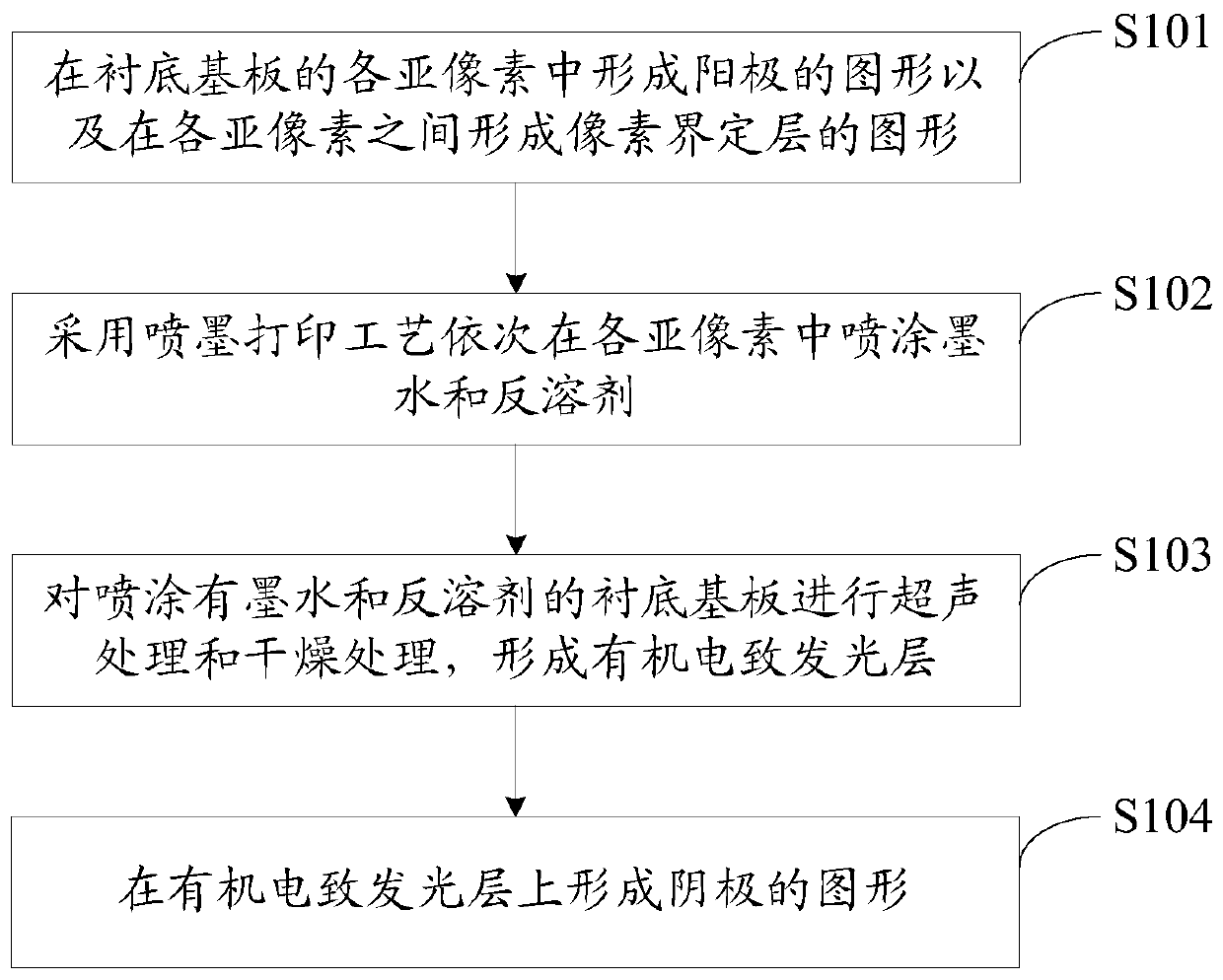
[0029] Embodiments of the present invention provide a method for preparing an electroluminescent display panel, such as figure 1 As shown, the preparation method may include the following steps:

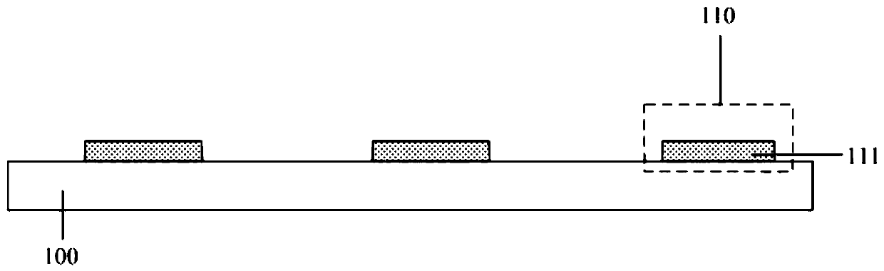
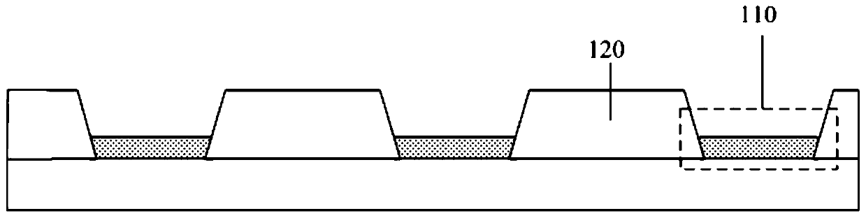
[0030] S101, forming a pattern of an anode in each sub-pixel of the base substrate and forming a pattern of a pixel defining layer between each sub-pixel.

[0031] Specifically, a single patterning process is used to form the patterns of the anodes in the sub-pixels of the base substrate. Wherein, the material of the anode may include a transparent conductive material. Wherein, the transparent conductive material may include one or a combination of indium tin oxide (ITO), indium zinc oxide (IZO), carbon nanotubes, graphene, nano gold and nano silver, which is not limited herein.

[0032] A patterning process is used to form the graphics of the pixel defining layer between the sub-pixels.

[0033] S102. Using an inkjet printing process to spray ink and anti-solvent in each sub-pixe...


PUM


Abstract

The invention discloses an electroluminescent display panel, its preparation method and a display device. By forming each anode in each sub-pixel of a base substrate and forming a pixel-defining layer between each sub-pixel, an inkjet printing process is used to print The anode of each sub-pixel is sprayed with ink and anti-solvent, and the base substrate sprayed with ink and anti-solvent is ultrasonically treated and dried to form an organic electroluminescent layer, and a cathode is formed on the organic electroluminescent layer to form an electroluminescent layer. Luminescent display panel. Since the inkjet printing process is used to spray ink and anti-solvent on the anode of each sub-pixel, the solute is precipitated by the principle that the anti-solvent and the solvent are mutually soluble and the solute is insoluble or slightly soluble in the anti-solvent. The solute is uniformly dispersed by ultrasonic treatment, and the solvent and anti-solvent are removed by drying treatment, so that the uniformity of the film thickness of the prepared organic electroluminescent layer is improved, and the coffee ring effect of the organic electroluminescent layer is avoided.

Description

technical field [0001] The invention relates to the field of display technology, in particular to an electroluminescence display panel, a preparation method thereof and a display device. Background technique [0002] Organic Light Emitting Diode (OLED) display has the advantages of low energy consumption, self-illumination, wide viewing angle and fast response speed. [0003] At present, the film-forming methods of the organic electroluminescent layer in OLED displays mainly include vapor deposition and inkjet printing. Among them, film formation by inkjet printing is considered to be an important way to achieve mass production of large-size OLED displays due to its fast film formation rate, high material utilization rate, and large-scale realization. Usually, when making an organic electroluminescent layer, it is necessary to pre-fabricate the anode and the pixel defining layer used to define the area where each sub-pixel is located on the substrate, and then use the inkje...

Claims


Application Information

Patent Timeline
Patent Type & Authority Patents(China)
IPC IPC(8): H01L51/50H01L51/56H01L27/32
CPCH10K59/30H10K71/135H10K50/11
Inventor 范招康
Owner BOE TECH GRP CO LTD
Why Eureka
Try Eureka