Manufacturing method of back of RC-IGBT device

A manufacturing method and device technology, applied in the fields of semiconductor/solid-state device manufacturing, semiconductor devices, electrical components, etc., can solve the problems of low activation efficiency, large debris risk, expensive equipment, etc., to improve the activation degree, increase the product process cost, Fragmentation rate reduction effect

Inactive Publication Date: 2018-08-21
无锡橙芯微电子科技有限公司
View PDF5 Cites 0 Cited by
  • Summary
  • Abstract
  • Description
  • Claims
  • Application Information

AI Technical Summary

Problems solved by technology

[0002] At present, there are two main ways to process the back of RC-IGBT. One is to use Taico technology to prepare ultra-thin sheets, and then do back injection to form N+buffer layer, N+ embedded layer and P+ hole injection layer (P+ layer layer). The liner process is used to bond the processed liner to the silicon substrate on the front side of the device, and then the positive film is thinned and implanted on the back to form an N+buffer layer, an N+ embedded layer an

Method used


Image

  • Manufacturing method of back of RC-IGBT device
  • Manufacturing method of back of RC-IGBT device
  • Manufacturing method of back of RC-IGBT device

Examples


Example Embodiment

[0038] The present invention will be further described below in conjunction with specific drawings and embodiments.

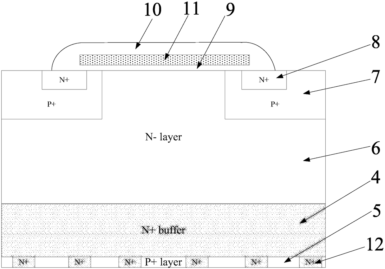
[0039] In the embodiment of the present invention, the method for fabricating the back surface of a planar gate RC-IGBT device is taken as an example for illustration, which is characterized in that it includes the following steps:

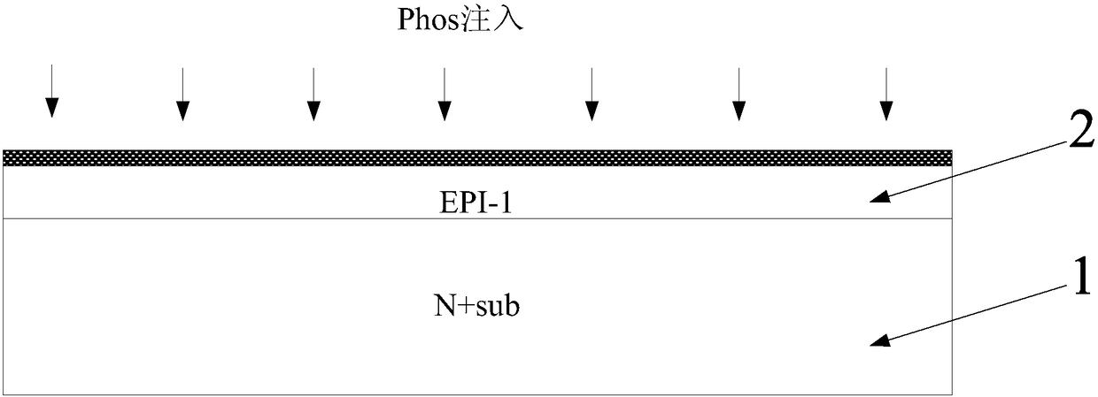
[0040] The first step: providing a semiconductor substrate, selecting an N-type semiconductor material as the semiconductor substrate 1, and the semiconductor substrate 1 is used as a support in the device manufacturing process;

[0041] like figure 2 As shown, the second step: on the semiconductor substrate 1, grow a first N-type epitaxial layer 2, the thickness of the first N-type epitaxial layer is 5-20 μm, and the resistivity is 40-100 ohm*cm;

[0042] like image 3 As shown, the third step: implanting N-type impurities on the surface of the first N-type epitaxial layer 2, where the N-type impurity ions are phosphorus, and t...


PUM


Abstract

The invention belongs to the technical field of manufacturing of a semi-conductor device, and relates to a manufacturing method of the back of an RC-IGBT device. A back technology is completed throughinjecting and high temperature annealing on the front of the RC-IGBT device. By means of the manufacturing method, the technology machining difficulty of the device can be effectively lowered, the fragment rate is lowered, and device parameters Vce are also increased; meanwhile, the manufacturing technology is compatible with the front of an existing IGBT, and the product technology cost is not increased.

Description

technical field [0001] The invention relates to a method for fabricating the back surface of an RC-IGBT (Reverse Conducting-IGBT, ie reverse conducting IGBT) device, belonging to the technical field of semiconductor device manufacturing. Background technique [0002] At present, there are two main ways to process the back of RC-IGBT. One is to use Taico technology to prepare ultra-thin sheets, and then do back injection to form N+buffer layer, N+ embedded layer and P+ hole injection layer (P+ layer layer). The liner process is used to bond the processed liner to the silicon substrate on the front side of the device, and then the positive film is thinned and implanted on the back to form an N+buffer layer, an N+ embedded layer and a P+ hole injection layer (P+ layer layer), and finally thermally peel off the positive film and the liner. The first method requires the use of Taico equipment, which is expensive and many foundries do not have this condition at present. Fragmenta...

Claims


Application Information

Patent Timeline
IPC IPC(8): H01L21/331H01L29/739
CPCH01L29/66333H01L29/7395
Inventor 张艳旺吴宗宪王宇澄
Owner 无锡橙芯微电子科技有限公司
Why Eureka
Try Eureka