an led chip

A technology of LED chip and reflective layer, applied in semiconductor devices, electrical components, circuits, etc., can solve the problem that the performance of LED chips needs to be improved, and achieve the effect of preventing abnormal leakage and improving performance.

Active Publication Date: 2019-08-23
ENRAYTEK OPTOELECTRONICS
View PDF6 Cites 0 Cited by
  • Summary
  • Abstract
  • Description
  • Claims
  • Application Information

AI Technical Summary

Problems solved by technology

[0005] The purpose of the present invention is to provide an LED chip to solve the problem that the performance of the LED chip needs to be improved in the prior art

Method used


Image

  • an led chip
  • an led chip
  • an led chip

Examples


Embodiment Construction

[0024] In order to make the objects, features and advantages of the present invention more comprehensible, please refer to the accompanying drawings. It should be noted that the structures, proportions, sizes, etc. shown in the drawings attached to this specification are only used to match the content disclosed in the specification, for those who are familiar with this technology to understand and read, and are not used to limit the implementation of the present invention. Limiting conditions, so there is no technical substantive meaning, any modification of structure, change of proportional relationship or adjustment of size, without affecting the effect and purpose of the present invention, should still fall within the scope of the present invention. The disclosed technical content must be within the scope covered.
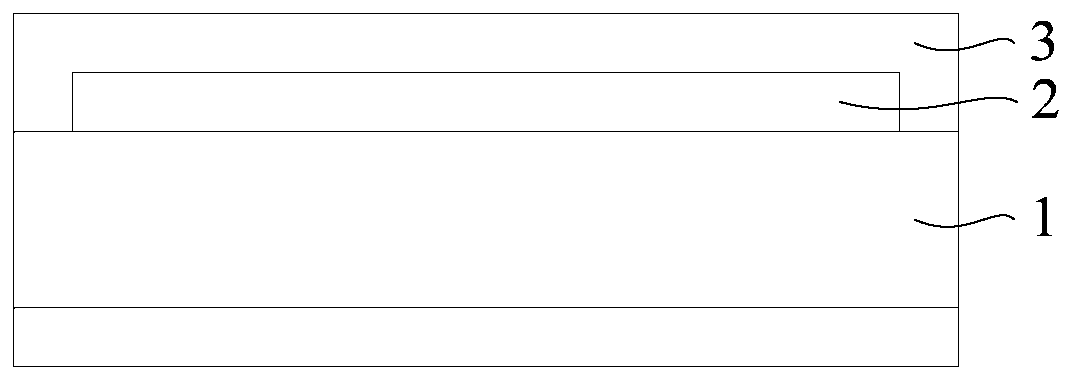
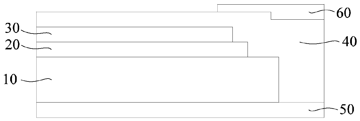
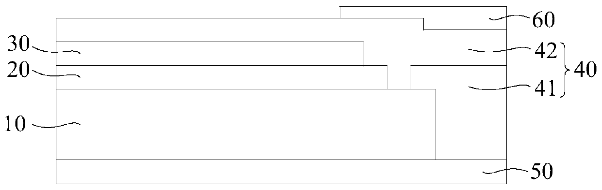
[0025] The core idea of ​​the present invention is to eliminate the adverse effects of "black bands" on the LED chip. However, if only the area of ​​the formed ...


PUM


Abstract

The invention provides an LED chip. The LED chip comprises a light-emitting diode, a reflecting layer, a blocking layer and an insulating layer, the light-emitting diode is located on a substrate, thereflecting layer is located on the light-emitting diode, the blocking layer is located on the reflecting layer, the reflecting layer and the blocking layer form a stair-shaped structure on the light-emitting diode, and the insulating layer covers the light-emitting diode, the reflecting layer and the blocking layer. By means of the LED chip, by making the reflecting layer located on the light-emitting diode and the blocking layer located on the reflecting layer form the stair-shaped structure, the area of the blocking layer is smaller than that of the reflecting layer, then through covering of the insulating layer, the phenomenon of a 'black zone' can be removed, metal in the reflecting layer can be prevented from expanding or migrating to the area of the light-emitting diode, an electricleakage abnormity is avoided, and the performance of the LED chip is improved.

Description

technical field [0001] The invention relates to the field of semiconductor manufacturing, in particular to an LED chip. Background technique [0002] Metal reflective layers are usually used in LED (Light Emitting Diode) chips to improve light reflectivity, but the metal in the reflective layer will undergo thermal diffusion and electromigration when heated and current passes, so in the chip manufacturing process A barrier layer (Barrier) that prevents metal diffusion will be used to completely cover the metal reflective layer, thereby preventing adverse effects caused by thermal diffusion and electromigration of the metal in the reflective layer, thereby better improving the reliability of the LED chip. [0003] However, in the prior art, such as figure 1 As shown, the reflective layer 2 on the light-emitting diode 1 is usually wrapped by the barrier layer 3, and there is a serious problem in the method of completely wrapping the barrier layer 3, because the reflectivity o...

Claims


Application Information

Patent Timeline
Patent Type & Authority Patents(China)
IPC IPC(8): H01L33/14H01L33/44H01L33/46
Inventor 朱秀山
Owner ENRAYTEK OPTOELECTRONICS
Why Eureka
Try Eureka