Organic light emitting display device and manufacturing method thereof
A light-emitting display and organic technology, applied in semiconductor/solid-state device manufacturing, electrical components, electric solid-state devices, etc., can solve the problems of low color gamut of organic light-emitting display and cannot meet people's needs, so as to improve color purity and reduce production cost , Improve the effect of display color gamut
- Summary
- Abstract
- Description
- Claims
- Application Information
AI Technical Summary
Problems solved by technology
Method used
Image

Examples
Embodiment approach
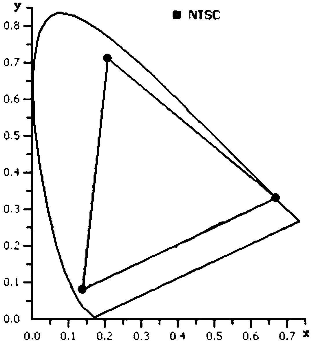
[0039] As an embodiment of the present invention, in this example, the microcavity optical path L of the green light unit G and luminescence wavelength λ G Satisfy the following formula: L G =n G lambda G , n Gis an integer greater than 2. Setting the first green light compensation layer and the second green light compensation layer can increase the length of the corresponding microcavity, that is, it can increase the distance of light propagating in the microcavity, so that the green light unit can realize a 3rd-order microcavity or a higher-order microcavity , which can effectively narrow the spectrum and increase the color gamut area.
[0040] At the same time, optionally, as another embodiment of the present invention, the microcavity optical path L of the red light unit R and luminescence wavelength λ R Satisfy the following formula: L R =n R lambda R , n G >n R >1,n R is an integer.
[0041] The microcavity optical path L specifically refers to the distance...
Embodiment 1
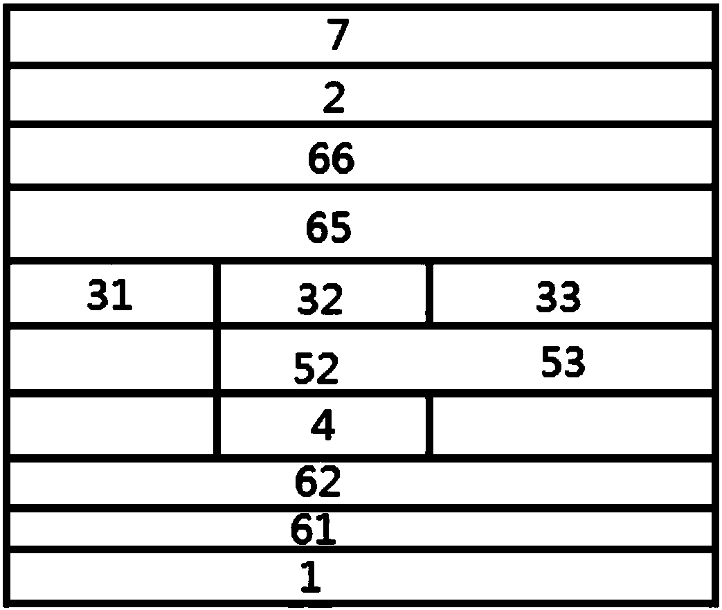
[0052] This embodiment provides an organic light emitting display device, such as image 3 As shown, it includes a first electrode layer 1 , a light-emitting layer and a second electrode layer 2 stacked up, and the light-emitting layer includes a red light unit 31 , a green light unit 32 , and a blue light unit 33 juxtaposed. The first electrode layer 1 is a reflective electrode layer, and the second electrode layer 2 is a transflective and semitransparent electrode layer. The first electrode layer 1 and the second electrode layer 2 and the space between them form a microcavity structure.
[0053] The organic light emitting display device further includes a first green light compensation layer 4 disposed between the green light unit 32 and the first electrode layer 1 . A hole injection layer 61 and a hole transport layer 62 are sequentially stacked between the first electrode layer 1 and the light emitting layer. The material of the first green light compensation layer 4 is t...
Embodiment 2
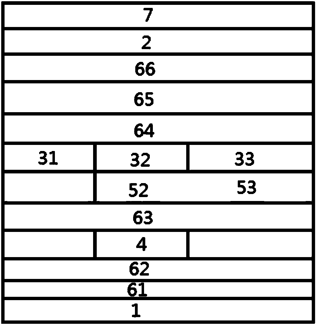
[0078] This embodiment provides an organic light-emitting display device, the device structure of which is the same as that of Embodiment 1, except that the second green light compensation layer 52 and the red light compensation layer 53 are not included.
[0079] The device structure of the red organic light-emitting diode in this embodiment is: ITO (10nm) / Ag (100nm) / ITO (10nm) / CuPc (20nm) / TPD (110nm) / CBP:Ir (piq) 3 (3%, 30nm) / TPBi(40nm) / LiF(1nm) / Mg:Ag(20%, 15nm) / NPB(60nm).
[0080]The device structure of the green organic light-emitting diode in this embodiment is: ITO (10nm) / Ag (100nm) / ITO (10nm) / CuPc (20nm) / TPD (110nm) / TPD (80nm) / CBP:Ir (ppy) 3 (10%, 30nm) / TPBi(40nm) / LiF(1nm) / Mg:Ag(20%, 15nm) / NPB(60nm).
[0081] The device structure of the blue light organic light emitting diode in the present embodiment is: ITO (10nm) / Ag (100nm) / ITO (10nm) / CuPc (20nm) / TPD (110nm) / CBP:DPVBi (3%, 30nm) / TPBi ( 40nm) / LiF(1nm) / Mg:Ag(20%, 15nm) / NPB(60nm).
PUM
| Property | Measurement | Unit |
|---|---|---|
| Thickness | aaaaa | aaaaa |
| Thickness | aaaaa | aaaaa |
| Thickness | aaaaa | aaaaa |
Abstract
Description
Claims
Application Information
 - R&D
- Intellectual Property
- Life Sciences
- Materials
- Tech Scout
- Unparalleled Data Quality
- Higher Quality Content
- 60% Fewer Hallucinations
Browse by: Latest US Patents, China's latest patents, Technical Efficacy Thesaurus, Application Domain, Technology Topic, Popular Technical Reports.
© 2025 PatSnap. All rights reserved.Legal|Privacy policy|Modern Slavery Act Transparency Statement|Sitemap|About US| Contact US: help@patsnap.com