Manufacturing method of PTFE-containing multilayered PCB

A technology of PTFE and its production method, which is used in multilayer circuit manufacturing, printed circuit manufacturing, electrical components, etc., can solve the problem of inability to effectively solve the problem of bonding force between PTFE multilayer boards and PP layers, increase the surface chemical activity of PTFE substrates, and cannot Better realize the combination of PTFE and adhesive sheet, etc., to save browning time, reduce residence time, and protect activity.

Inactive Publication Date: 2018-08-24
GUANGDONG SHENGYI SCI TECH
View PDF6 Cites 3 Cited by
  • Summary
  • Abstract
  • Description
  • Claims
  • Application Information

AI Technical Summary

Problems solved by technology

[0006] Although the above-mentioned documents have disclosed the use of low-temperature plasma treatment or the layered structure of combining PTFE film and inverted copper foil through FEP film to achieve the purpose of low-temperature lamination, it still cannot maximize and maintain the surface of the PTFE substrate. Therefore, the combination between PTFE and adhesive sheet cannot be better realized, and the problem of interlayer bonding between PTFE multilayer board and PP cannot be effectively solved.

Method used


Image

  • Manufacturing method of PTFE-containing multilayered PCB
  • Manufacturing method of PTFE-containing multilayered PCB

Examples

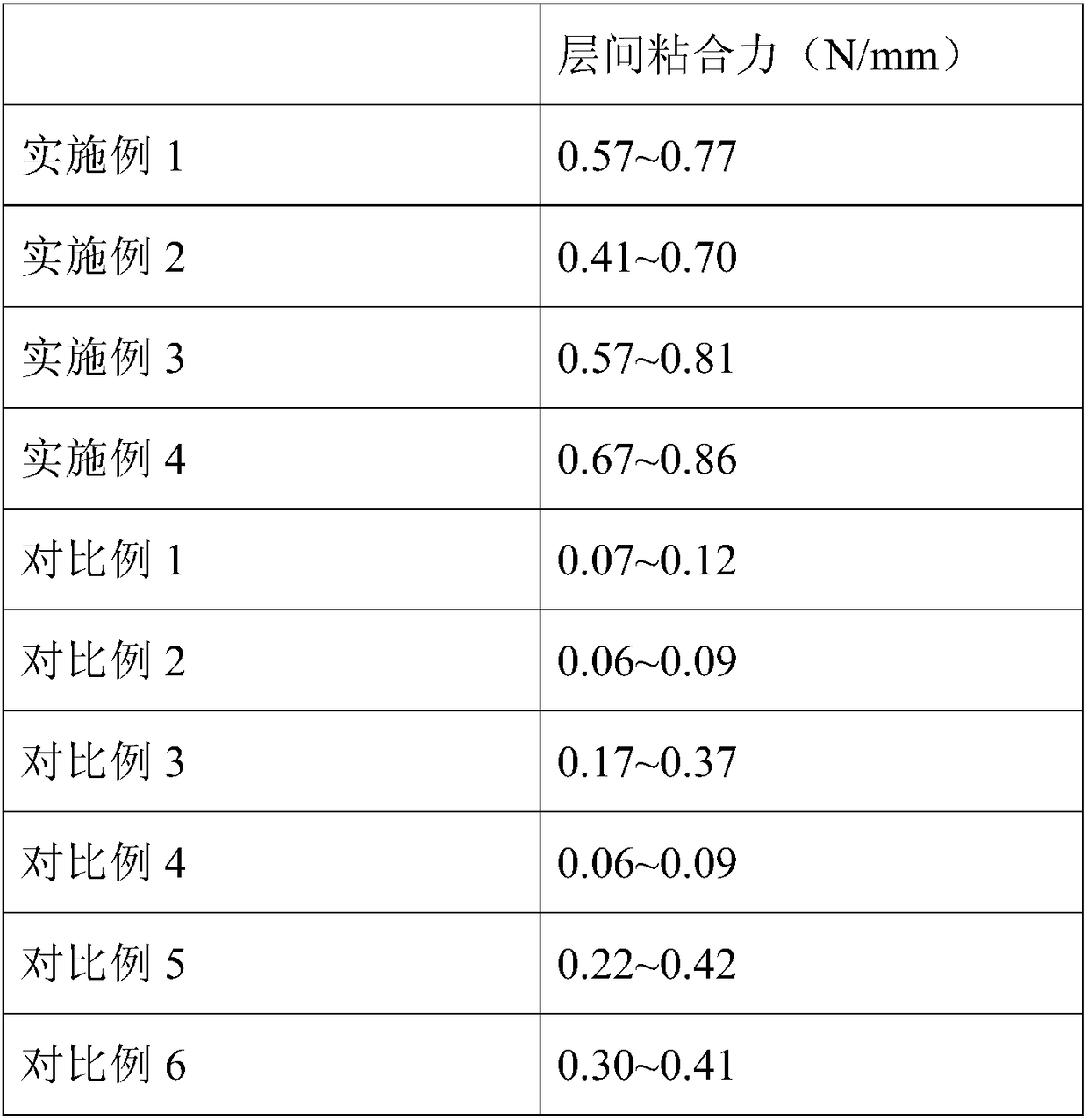

Embodiment 1

[0044] A kind of manufacture method that contains the multilayer PCB of PTFE, it comprises the following steps:

[0045] (1) Provide PTFE substrate with RTF copper foil, without any form of grinding and micro-etching after cutting;

[0046] (2) Etching the circuit, the PTFE substrate after etching the circuit is not browned;

[0047] (3) do plasma surface plasma activation treatment on the PTFE substrate surface after etching, the temperature of said plasma surface plasma activation treatment is controlled at 50 ℃, and the time is controlled at 1h;

[0048] The plasma surface activation treatment of the plasma is specifically: the first step adopts O 2 , N 2 and H 2 The gas is treated with a volume ratio of 10:10:20, under the pressure of 250 Torr, and the plasma gas flow rate is 2.5LT / min for 15 minutes; the second step uses N 2 and H 2 The gas was treated for 45 minutes at a volume ratio of 20:80 under a pressure of 250 Torr and a plasma flow rate of 2.5 LT / min;

[004...

Embodiment 2

[0052] A kind of manufacture method that contains the multilayer PCB of PTFE, it comprises the following steps:

[0053] (1) Provide PTFE substrate with RTF copper foil, without any form of grinding and micro-etching after cutting;

[0054] (2) Etching the circuit, the PTFE substrate after etching the circuit is not browned;

[0055] (3) do plasma surface plasma activation treatment on the PTFE substrate surface after etching, the temperature of described plasma surface plasma activation treatment is controlled at 40 ℃, and the time is controlled at 50min;

[0056] The plasma surface activation treatment of the plasma is specifically: the first step adopts O 2 , N 2 and H 2 The gas is treated for 15 minutes at a volume ratio of 10:10:20 under a pressure of 220 Torr and a plasma gas flow rate of 3LT / min; the second step uses N 2 and H 2 The gas was treated for 35 minutes at a volume ratio of 20:80 under a pressure of 250 Torr and a plasma flow rate of 2.5 LT / min;

[0057]...

Embodiment 3

[0060] A kind of manufacture method that contains the multilayer PCB of PTFE, it comprises the following steps:

[0061] (1) Provide PTFE substrate with RTF copper foil, without any form of grinding and micro-etching after cutting;

[0062] (2) Etching the circuit, the PTFE substrate after etching the circuit is not browned;

[0063] (3) do plasma surface plasma activation treatment on the PTFE substrate surface after etching, the temperature of said plasma surface plasma activation treatment is controlled at 30 ℃, and the time is controlled at 40min;

[0064] The plasma surface activation treatment of the plasma is specifically: the first step adopts O 2 , N 2 and H 2 The gas was treated for 10 minutes at a volume ratio of 10:10:40 under a pressure of 250 Torr and a plasma flow rate of 3LT / min; the second step was to use N 2 and H 2 The gas was treated for 30 minutes at a volume ratio of 20:40 under a pressure of 220 Torr and a plasma flow rate of 2.5 LT / min;

[0065] (...


PUM


Abstract

The invention relates to a manufacturing method of a PTFE-containing multilayered PCB. The manufacturing method comprises the following steps of (1) providing a PTFE substrate adopting an RTF copper coil; (2) performing circuit etching, and not forming a brown line on the circuit-etched PTFE substrate; (3) performing plasma surface plasma activation treatment on the surface of the etched PTFE substrate; (4) performing a laminating procedure, and controlling the residence time before lamination to be within 4h; and (5) completing lamination to obtain the PTFE-containing multilayered PCB. By adjusting the PCB design, the technological flows and the involved parameters, the interlayer adhesive force between PP and the substrate is increased to the maximum degree, thereby solving the problem of adhesive force between the PTFE multilayered board and PP.

Description

technical field [0001] The invention relates to the technical field of copper clad laminates, in particular to a method for manufacturing a multilayer board containing PTFE. Background technique [0002] With the advent of the 5G era, more and more PTFE substrates are used in the wireless communication industry. The general 5G base station antenna PCB design is a four-layer laminate, which usually uses a four-layer board from top to bottom: PTFE substrate, bonding sheet, bonding sheet, and PTFE substrate. In addition, it also includes PTFE The multi-layer board design of the material all puts forward requirements for the adhesion between the PTFE substrate and the adhesive sheet. [0003] PTFE itself has very low surface energy and has non-stick properties; the contact angle is very large, so it cannot be bonded to any adhesive sheet. Therefore, how to improve the adhesion of PTFE surface is a hot issue in this field. [0004] CN106268370A discloses a treatment method for ...

Claims


Application Information

Patent Timeline
Patent Type & Authority Applications(China)
IPC IPC(8): H05K3/46
CPCH05K3/4611H05K2203/095
Inventor 赖罗鲁羲
Owner GUANGDONG SHENGYI SCI TECH
Why Eureka
Try Eureka