

Polypyrrole surface-modified one-dimensional silicon-based gas-sensing material and preparation method thereof
A technology for surface modification and gas-sensing materials, applied in the field of room-temperature working gas-sensing materials, can solve the problems of limited application and low sensitivity, and achieve the effects of improving diffusion capacity, increasing sensitivity, and reducing working temperature
- Summary
- Abstract
- Description
- Claims
- Application Information
AI Technical Summary
Problems solved by technology
Method used
Image

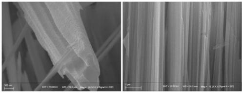
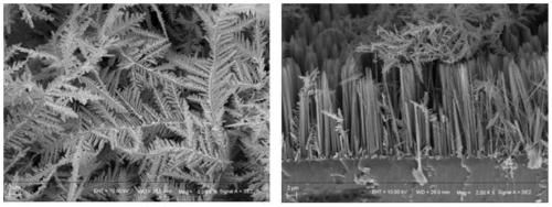
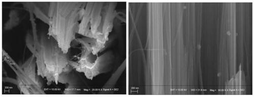
Examples
Embodiment 1
[0032] (1) Cleaning of monocrystalline silicon wafers
[0033] Silicon wafers were ultrasonically cleaned in hydrogen peroxide (10wt% hydrogen peroxide aqueous solution) and concentrated sulfuric acid (98wt% by mass) at a volume ratio of 4:1 for 10 minutes, and then placed in acetone solvent, absolute ethanol, and deionized water successively. Ultrasonic cleaning was performed for 5-10 minutes to remove surface oil and organic impurities, and then dried thoroughly in an infrared oven.
[0034] (2) Configure chemical etching solution
[0035] Dissolving silver nitrate in hydrofluoric acid aqueous solution, the concentration of hydrofluoric acid in the obtained solution is 5M, and the concentration of silver nitrate is 0.025M. (3) Metal-assisted chemical etching
[0036] Putting the silicon wafer into the solution prepared in step (2) for etching, the etching time is 150 min.
[0037] (4) Clean the etched silicon wafer
[0038] After the silicon chip obtained in step (3) is ...
Embodiment 2
[0050] (1) Cleaning of monocrystalline silicon wafers
[0051] Silicon wafers were ultrasonically cleaned in hydrogen peroxide (10wt% hydrogen peroxide aqueous solution) and concentrated sulfuric acid (98wt% by mass) at a volume ratio of 4:1 for 10 minutes, and then placed in acetone solvent, absolute ethanol, and deionized water successively. Ultrasonic cleaning was performed for 5-10 minutes to remove surface oil and organic impurities, and then dried thoroughly in an infrared oven.
[0052] (2) Configure chemical etching solution
[0053] Dissolving silver nitrate in hydrofluoric acid aqueous solution, the concentration of hydrofluoric acid in the obtained solution is 3M, and the concentration of silver nitrate is 0.02M.
[0054] (3) Metal-assisted chemical etching
[0055] Putting the silicon wafer into the solution prepared in step (2) for etching, the etching time is 180 min.
[0056] (4) Clean the etched silicon wafer
[0057] After the silicon chip obtained in step...
Embodiment 3
[0069] (1) Cleaning of monocrystalline silicon wafers
[0070] Silicon wafers were ultrasonically cleaned in hydrogen peroxide (10wt% hydrogen peroxide aqueous solution) and concentrated sulfuric acid (98wt% by mass) at a volume ratio of 4:1 for 10 minutes, and then placed in acetone solvent, absolute ethanol, and deionized water successively. Ultrasonic cleaning was performed for 5-10 minutes to remove surface oil and organic impurities, and then dried thoroughly in an infrared oven.
[0071] (2) Configure chemical etching solution
[0072] Dissolving silver nitrate in hydrofluoric acid aqueous solution, the concentration of hydrofluoric acid in the obtained solution is 6M, and the concentration of silver nitrate is 0.03M.
[0073] (3) Metal-assisted chemical etching
[0074] Putting the silicon wafer into the solution prepared in step (2) for etching, the etching time is 90 minutes.
[0075] (4) Clean the etched silicon wafer
[0076] After the silicon chip obtained in s...
PUM
| Property | Measurement | Unit |
|---|---|---|
| thickness | aaaaa | aaaaa |
| thickness | aaaaa | aaaaa |
| thickness | aaaaa | aaaaa |
Abstract
Description
Claims
Application Information