
Method for epitaxially growing large chamfering angle sapphire substrate-based GaN and application of GaN

A sapphire substrate and epitaxial growth technology, which is applied in the direction of electrical components, semiconductor/solid-state device manufacturing, circuits, etc., can solve the problems of poor luminous intensity and half-width, GaN steps coalescing, and low crystal quality, so as to overcome the steps Agglomeration phenomenon, easy application, effect of improving material quality

Inactive Publication Date: 2018-09-07
SUZHOU INST OF NANO TECH & NANO BIONICS CHINESE ACEDEMY OF SCI +1
View PDF6 Cites 2 Cited by
  • Summary
  • Abstract
  • Description
  • Claims
  • Application Information

AI Technical Summary

Problems solved by technology

However, the bevel angle of the current commercial sapphire substrate is generally 0.2°, because a larger bevel angle will cause serious step aggregation of GaN grown on it, which will affect its use.
Therefore, the current GaN growth process is optimized for small bevel angle (0.2°) sapphire substrates, and the crystal quality of InGaN grown on small bevel angles is not high, and the luminous intensity and half width are not good.

Method used


Image

  • Method for epitaxially growing large chamfering angle sapphire substrate-based GaN and application of GaN
  • Method for epitaxially growing large chamfering angle sapphire substrate-based GaN and application of GaN
  • Method for epitaxially growing large chamfering angle sapphire substrate-based GaN and application of GaN

Examples


Embodiment Construction

[0031] Hereinafter, embodiments of the present invention will be described in detail with reference to the accompanying drawings. This invention may, however, be embodied in many different forms and should not be construed as limited to the specific embodiments set forth herein. Rather, the embodiments are provided to explain the principles of the invention and its practical application, thereby enabling others skilled in the art to understand the invention for various embodiments and with various modifications as are suited to particular intended uses.

[0032] It will be understood that although the terms "first", "second", etc. may be used herein to describe various substances, these substances should not be limited by these terms. These terms are only used to distinguish one substance from another.

[0033] Based on the use of large off-cut angle (greater than 0.2°) sapphire substrates, it is easier to achieve step flow growth to obtain high-quality green or yellow band I...


PUM

PropertyMeasurementUnit
Thicknessaaaaaaaaaa
Thicknessaaaaaaaaaa
Thicknessaaaaaaaaaa

Abstract

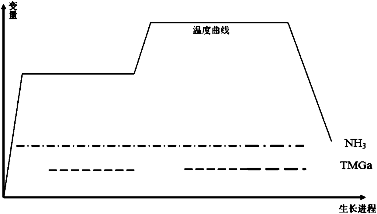
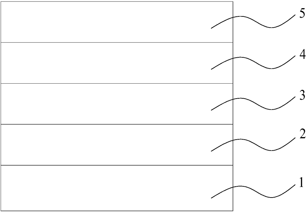
The invention provides a method for epitaxially growing large chamfering angle sapphire substrate-based GaN. The method comprises the steps of S1, placing a large chamfering angle sapphire substrate with a chamfering angle larger than 0.2 degree in an epitaxial growth device, and sequentially growing a nucleating layer ,an unintentionally-doped GaN layer and a first layer of n-type GaN on the large chamfering angle sapphire substrate in a lamination way; and S2, introducing NH3 and trimethyl gallium into the epitaxial growth device, controlling the flowing ratio of the NH3 and the trimethyl gallium to be larger than 600, and simultaneously controlling chamber pressure of the epitaxial growth device to be smaller than 400mbar so that a second layer of n-type GaN is grown on the first layerof n-type GaN at a speed larger than 0.5 nanometer per second and a large chamfering angle sapphire substrate-GaN composite structure is obtained. By optimizing a growth process, high-quality GaN is epitaxially grown on the large chamfering angle sapphire substrate, so that grown on a template of the large chamfering angle sapphire substrate-GaN composite structure can be performed to obtain a high-quality green-light or yellow-light waveband InGaN quantum well.

Description

technical field [0001] The invention belongs to the technical field of semiconductors, and specifically relates to a method for epitaxially growing gallium nitride on a sapphire substrate with a large off-cut angle and its application. Background technique [0002] The sapphire substrate is a commonly used substrate in the current LED (light emitting diode) or LD (laser diode) industry. It is cheap and has mature technology. Compared with the expensive GaN self-supporting substrate, it is more widely used. By epitaxially growing a section of GaN on a sapphire substrate, a GaN substrate that can be used for InGaN growth is obtained. This sapphire-gallium nitride composite structure is called a template, which can be used for subsequent light-emitting device fabrication. The template obtained by growing GaN epitaxially on the bottom is an indispensable technology in the LED and LD industries. [0003] In addition, InGaN is the core material that constitutes the quantum wells ...

Claims


Application Information

Patent Timeline
IPC IPC(8): H01L21/02H01L33/00
CPCH01L21/0242H01L21/02428H01L21/02458H01L21/0254H01L21/0262H01L33/0066H01L33/0075
Inventor 江灵荣刘建平田爱琴杨辉
Owner SUZHOU INST OF NANO TECH & NANO BIONICS CHINESE ACEDEMY OF SCI
Learn More