Organic electroluminescent device

An electroluminescence device and electroluminescence technology, which are applied to circuits, electrical components, electric solid devices, etc., can solve the problem of insufficient color gamut of OLED devices, and achieve the effect of improving luminous efficiency and utilization rate

Active Publication Date: 2018-09-07
YUNGU GUAN TECH CO LTD
View PDF7 Cites 5 Cited by
  • Summary
  • Abstract
  • Description
  • Claims
  • Application Information

AI Technical Summary

Problems solved by technology

[0006] For this reason, the technical problem to be solved by the present invention is that in the prior art, the color gamut of OLED devices is not high enough

Method used


Image

  • Organic electroluminescent device
  • Organic electroluminescent device
  • Organic electroluminescent device

Examples


Embodiment 1

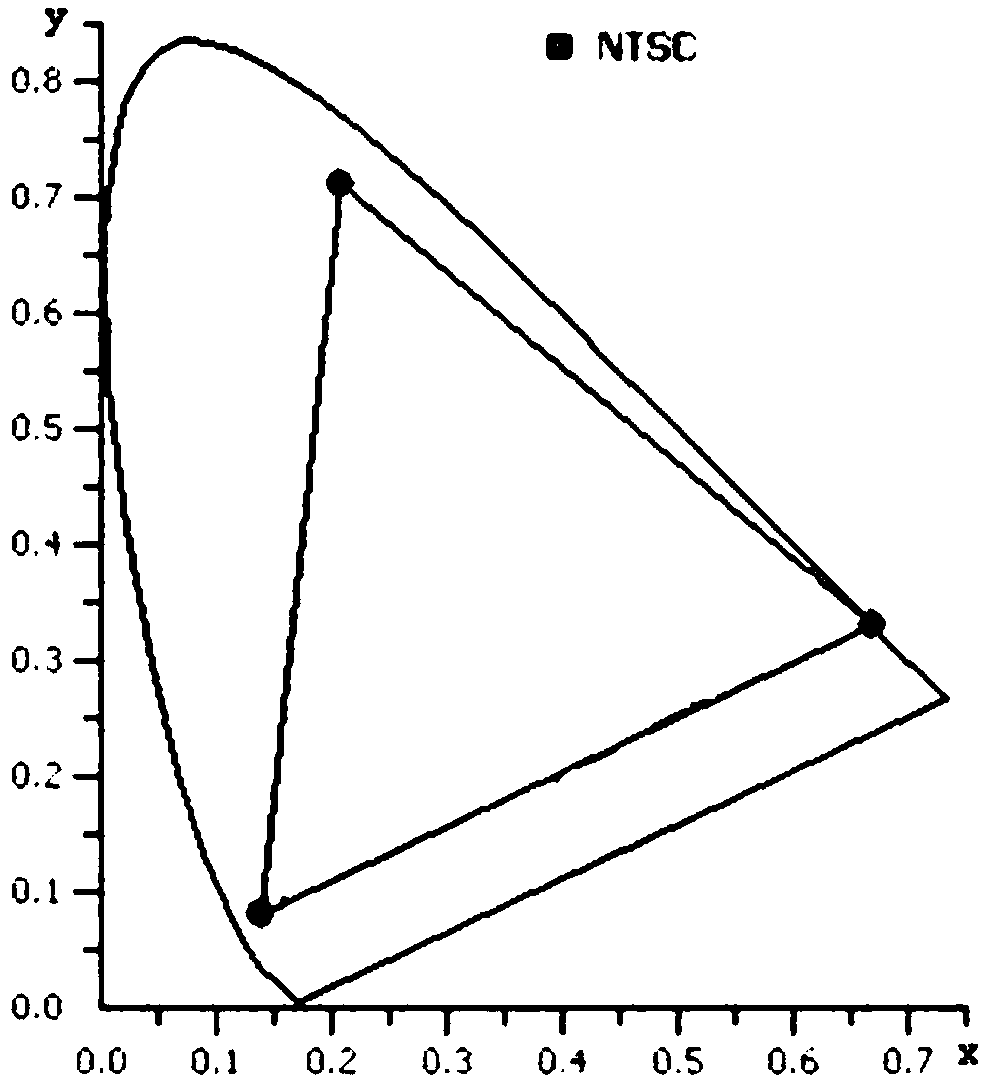
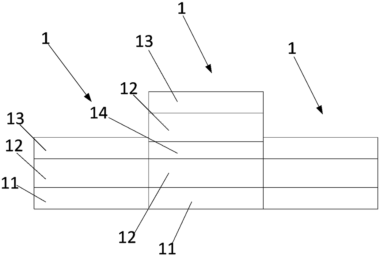
[0089] The embodiment of the present invention provides a specific example of an organic electroluminescence device. The organic electroluminescent device in this embodiment includes monochromatic organic light emitting diodes with three light emitting wavelengths, namely red organic light emitting diodes, green light organic light emitting diodes and blue light organic light emitting diodes. Among them, the three organic light emitting diodes all have a microcavity structure.

[0090] Each organic light emitting diode includes a first electrode layer, a light emitting layer and a second electrode layer which are stacked. Wherein, there are two light-emitting layers in the green organic light-emitting diode, and the two light-emitting layers are connected through a transparent connection layer, and the transparent connection layer is Li 2 CO 3 / HAT-CN / TAPC with a thickness of 50nm and a refractive index of 1.8. Blue light and red light organic light emitting diodes each hav...

Embodiment 2

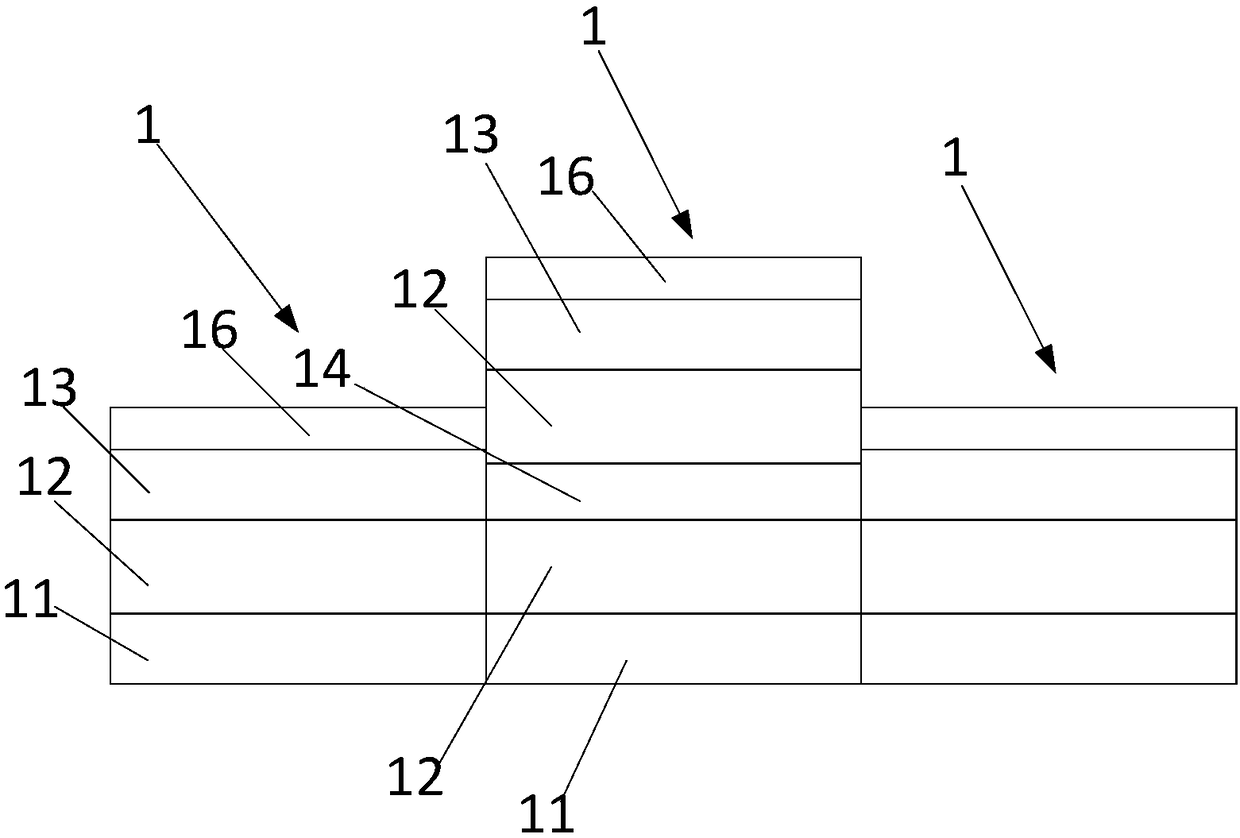
[0098] The embodiment of the present invention provides a specific example of an organic electroluminescence device. Its structure is the same as embodiment 1, and the difference with the organic electroluminescent device that embodiment 1 provides is:

[0099] Both red and green OLEDs have two light-emitting layers, and blue OLEDs have one light-emitting layer.

[0100] The device structure of the red organic light-emitting diode in this embodiment is: ITO (10nm) / Ag (100nm) / ITO (10nm) / CuPc (20nm) / TPD (70nm) / CBP:Ir (piq) 3 (3%,30nm) / TPBi(40nm) / Li 2 CO 3 (1nm) / HAT-CN(10nm) / CuPc(20nm) / TPD(70nm) / CBP:Ir(piq) 3 (3%, 30nm) / TPBi(40nm) / LiF(1nm) / Mg:Ag(20%, 15nm) / NPB(60nm).

Embodiment 3

[0102] The embodiment of the present invention provides a specific example of an organic electroluminescence device. Its structure is the same as that of Embodiment 1, and the difference from the organic electroluminescence device provided by Embodiment 1 lies in that the thickness of the hole transport layer in the green organic light emitting diode is different.

[0103] The device structure of the green organic light-emitting diode in this embodiment is: ITO (10nm) / Ag (100nm) / ITO (10nm) / CuPc (20nm) / TPD (30nm) / CBP:Ir (ppy) 3 (10%,30nm) / TPBi(40nm) / Li 2 CO3(1nm) / HAT-CN(10nm) / CuPc(20nm) / TPD(30nm) / CBP:Ir(ppy) 3(3%,30nm) / TPBi(40nm) / LiF(1nm) / Mg:Ag(20%,15nm) / NPB(60nm)


PUM


Abstract

The invention relates to the field of display technology, and discloses an organic electroluminescent device. The organic electroluminescent device comprises a single-color organic light-emitting diode with m different light-emitting wavelengths or a white light organic light-emitting diode provided with an optical filter, wherein at least one organic light-emitting diode with a micro-cavity structure light-emitting wavelength comprises at least two light-emitting layers; the microcavity optical path L of the organic light-emitting diode with the micro-cavity structure and light-emitting wavelength lambda of the corresponding light-emitting unit meet the following relation: L is equal to nlambda, wherein n is larger than or equal to 2, and n is a positive integer; n correspondingto at least one organic light-emitting diode is larger than or equal to 3; i is less than or equal to m and larger than or equal 1; and i and m are positive integers. The organic light-emitting diodewith the microcavity structure is characterized in that n-stage micro cavity effect can be realized, and n is a positive integer which is larger than and equal to 2, so that a two-order microcavity, athree-order microcavity, a four-order microcavity or a higher-order microcavity can be realized; the microcavity effect is enhanced; the spectrum is narrowed further; and the color range area is increased further.

Description

technical field [0001] The invention relates to the field of display technology, in particular to an organic electroluminescent device. Background technique [0002] Organic electroluminescence display (English full name Organic Light Emitting Display, referred to as OLED) is an active light-emitting display device, due to its advantages of high contrast, wide viewing angle, low power consumption, thinner volume, etc. It is prepared by a roll to roll process and is easy to realize flexible display, which is one of the most concerned technologies in the current flat panel display technology. [0003] With the continuous development of OLED technology, higher and higher requirements are placed on the performance of display devices. For example, increasing the color gamut, etc. The so-called color gamut is a method of encoding a color, and also refers to the sum of colors that a technical system can produce. figure 1 It is a color coordinate diagram formulated by NTSC (Natio...

Claims


Application Information

Patent Timeline
Patent Type & Authority Applications(China)
IPC IPC(8): H01L51/50H01L51/52
CPCH10K50/13H10K50/125H10K50/852
Inventor 周小康张浩杰逄辉何麟李梦真魏金贝李田田金世遇李维维李国孟田景文
Owner YUNGU GUAN TECH CO LTD
Why Eureka
Try Eureka