
Pixel structure, array substrate and display device

A pixel structure and array substrate technology, applied in the direction of diodes, semiconductor devices, electrical components, etc., can solve problems such as increasing power consumption, affecting user viewing distance experience, and color deviation in pixel areas, so as to optimize color deviation and improve light source utilization rate, improve the effect of color deviation

Active Publication Date: 2018-09-14
BOE TECH GRP CO LTD +1
View PDF5 Cites 4 Cited by
  • Summary
  • Abstract
  • Description
  • Claims
  • Application Information

AI Technical Summary

Problems solved by technology

Due to various factors such as patent barriers, it is difficult to design the current pixel into a symmetrical structure, which will also lead to asymmetrical color casts at different angles at the same angle, for example: one side of the screen is blue, and the other side is pink
This will seriously affect the user's visual experience
[0004] Therefore, in the process of implementing the present application, the inventors found that there are at least the following problems in the prior art: the current pixel structure, especially the asymmetric pixel structure, has light leakage phenomenon and the light leakage on both sides is asymmetrical, resulting in color on both sides of the pixel area. Deviation, which seriously affects the user's line-of-sight experience
In addition, light leakage will also affect the efficiency of the light source and increase power consumption

Method used


Image

  • Pixel structure, array substrate and display device
  • Pixel structure, array substrate and display device
  • Pixel structure, array substrate and display device

Examples


Embodiment Construction

[0023] In order to make the object, technical solution and advantages of the present invention clearer, the present invention will be described in further detail below in conjunction with specific embodiments and with reference to the accompanying drawings.

[0024] It should be noted that all expressions using "first" and "second" in the embodiments of the present invention are to distinguish two entities with the same name but different parameters or parameters that are not the same, see "first" and "second" It is only for the convenience of expression, and should not be construed as a limitation on the embodiments of the present invention, which will not be described one by one in the subsequent embodiments.

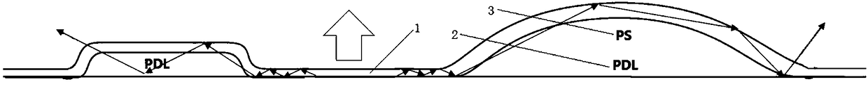
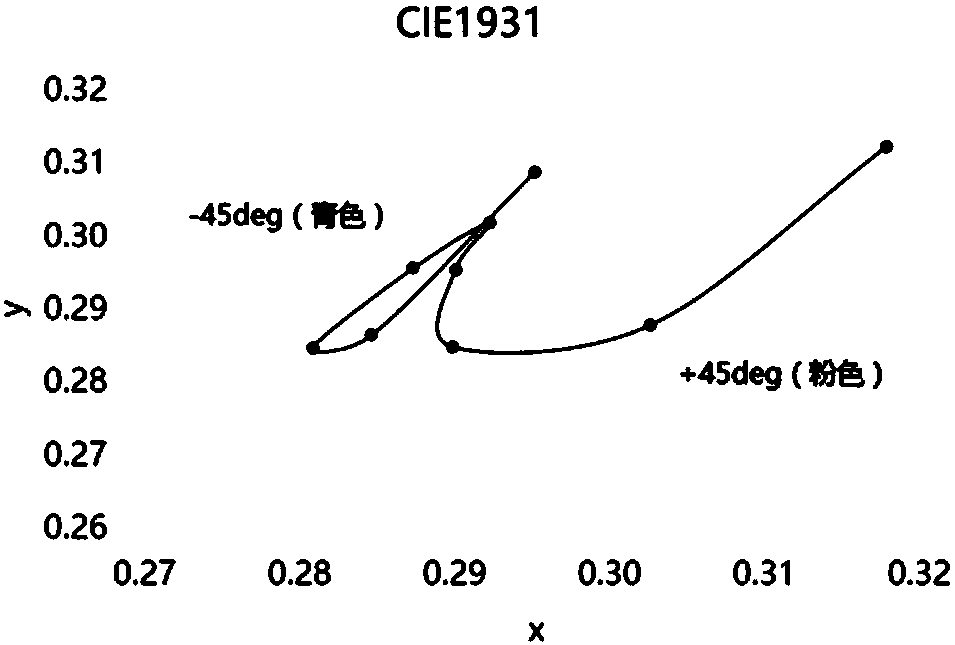
[0025] Based on the existing light leakage problem and the corresponding color deviation problem brought to users, the present application proposes an improved structure, which can avoid the occurrence of the above problems.

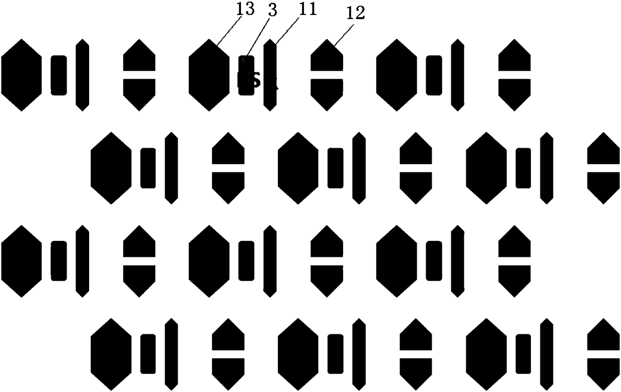
[0026] First, refer to figure 1 As shown...


PUM


Abstract

The invention discloses a pixel structure, an array substrate and a display device. The pixel structure includes subpixel units which is arranged in an array, pixel defining layers of which are located at two sides of each subpixel unit, and spacers which are arranged on the pixel defining layers, wherein the spacers are used for reflecting the light outward from two sides of each subpixel unit tothe areas in which the subpixel units are located. The pixel structure can reflect back the light leaked from two sides of each subpixel unit so as to avoid the light leakage phenomenon on both sidesof the pixel unit, by setting the pixel-defining layers on both sides of each subpixel unit and forming the spacers having a reflective effect on the light-emitting areas on both sides of each subpixel unit. The pixel structure, the array substrate and the display device can reduce light leakage at two sides of the pixel unit, can improve the problem that two sides of the pixel unit has color deviation caused by light leakage, and can improve the utilization rate of the light source and reduce power consumption at the same time.

Description

technical field [0001] The present invention relates to the technical field related to liquid crystal display, in particular to a pixel structure, an array substrate and a display device. Background technique [0002] At present, with the rapid application and development of display devices, the requirements for display devices are correspondingly higher and higher, especially for the consideration of user experience, more attention will be paid to the user's visual experience. For example, the currently popular organic light emitting diode (Organic Light Emitting Diode, OLED) device is a type of device that makes organic materials emit light under the action of an electric field. Therefore, OLED has high contrast, can achieve ultra-thin flexibility, short response time, etc. features. At present, OLED display lighting technology is developing by leaps and bounds. While meeting the individual needs of users, it also exposes some problems. The most prominent problem is that ...

Claims


Application Information

Patent Timeline
IPC IPC(8): H01L27/32
CPCH10K59/50H10K59/122
Inventor 周威龙
Owner BOE TECH GRP CO LTD
Features
  • Generate Ideas
  • Intellectual Property
  • Life Sciences
  • Materials
  • Tech Scout
  • Unparalleled Data Quality
  • Higher Quality Content
  • 60% Fewer Hallucinations
Learn More