Detector integrated array structure and detector receiving module

A detector array and array structure technology, which is applied in electromagnetic receivers, electric solid-state devices, semiconductor devices, etc., can solve problems such as limited packaging space of detector arrays, crosstalk of cables, and influence on device performance, so as to reduce design difficulty, The effect of reducing crosstalk and small size

Inactive Publication Date: 2018-09-14
INST OF SEMICONDUCTORS - CHINESE ACAD OF SCI
View PDF5 Cites 4 Cited by
  • Summary
  • Abstract
  • Description
  • Claims
  • Application Information

AI Technical Summary

Problems solved by technology

In the detector integrated array package, since there are many components used in the detector bias circuit, and the detector array package space is limited, the bias circuit and the radio frequency circuit are designed on the same plane at the same time in the prior art. Cables often introduce crosstalk and affect device performance, so the design of the microwave circuit in the detector integrated array module has become a technical difficulty

Method used


Image

  • Detector integrated array structure and detector receiving module
  • Detector integrated array structure and detector receiving module
  • Detector integrated array structure and detector receiving module

Examples


Embodiment Construction

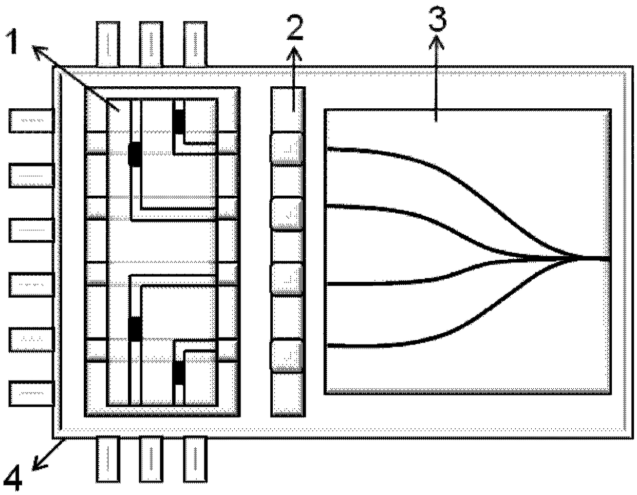
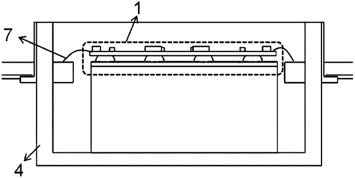
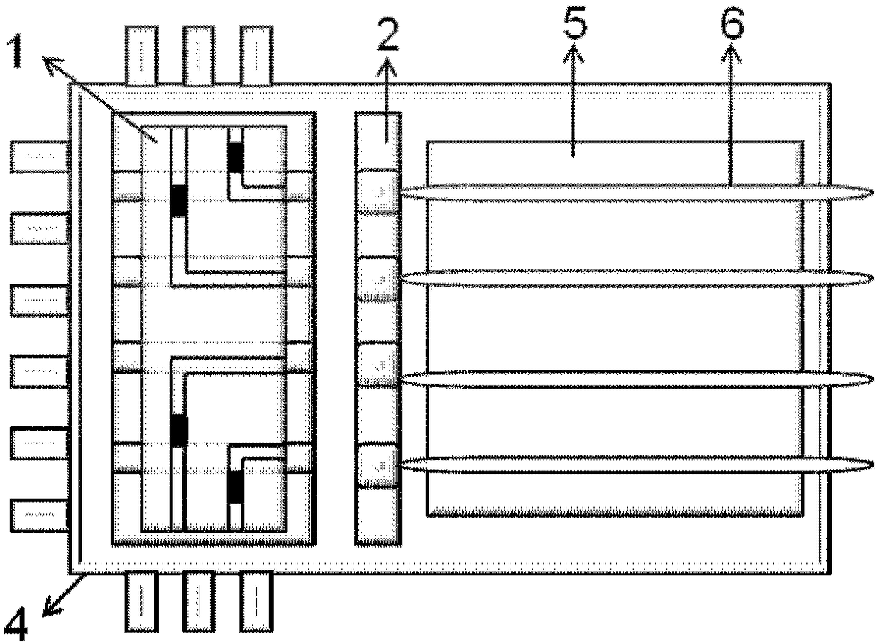
[0029] The disclosure provides a detector integrated array structure and a detector receiving module. By setting the microwave circuit into a three-dimensional microwave circuit, the three-dimensional microwave circuit includes two layers of circuit boards, and the upper circuit board is used as a DC bias circuit. , the lower circuit board is used as a high-frequency circuit, and components can be mounted on the upper and lower circuit boards, and the high-frequency circuit and the bias circuit are separated in physical space, which effectively utilizes the internal space of the array structure and reduces the internal space. The design difficulty of the circuit reduces the crosstalk between the circuits, has the advantages of simple structure, small size and high integration, and can be applied to a large-capacity communication system.

[0030] In order to make the purpose, technical solutions and advantages of the present disclosure clearer, the present disclosure will be fur...


PUM


Abstract

The invention discloses a detector integrated array structure and a detector receiving module, wherein the detector integrated array structure comprises: a light incident interface used for accessingan optical signal; a detector array chip set corresponding to the light incident interface and used for converting the optical signal into an electrical signal; and a three-dimensional microwave circuit containing two layers of circuit boards physically spaced apart, wherein one layer of the circuit board contains a bias circuit for providing a reverse bias voltage to the detector chip array, andthe other layer of the circuit board contains a high frequency circuit for transmitting the electrical signal output by the detector array chip to the outside of the detector integrated array structure. The structure separates the high frequency circuit and the bias circuit in the physical space, which effectively utilizes the internal space of the array structure, reduces the design difficulty ofthe internal circuit, and reduces the crosstalk between the circuits. The invention has the advantages of simple structure, small size as well as high integration degree, and is suitable for large-capacity communication systems.

Description

technical field [0001] The disclosure belongs to the field of optical communication devices, and relates to a detector integrated array structure and a detector receiving module. Background technique [0002] With the rapid growth of broadband traffic, optical communication devices are developing toward integration, large capacity, small size, and high speed. The development trend of high integration makes array integration a research hotspot. [0003] The detector receiving module is the core part of the optical fiber communication network, and its structure directly determines the performance of the device. In the detector integrated array package, since there are many components used in the detector bias circuit, and the detector array package space is limited, the bias circuit and the radio frequency circuit are designed on the same plane at the same time in the prior art. Cables often introduce crosstalk and affect device performance, so the design of the microwave ci...

Claims


Application Information

Patent Timeline
Patent Type & Authority Applications(China)
IPC IPC(8): H04B10/60H01L27/146
CPCH01L27/14601H04B10/60
Inventor 赵泽平刘建国刘宇张志珂
Owner INST OF SEMICONDUCTORS - CHINESE ACAD OF SCI
Why Eureka
Try Eureka