
Detector and emission imaging device having same

A technology of imaging equipment and detectors, which is applied in the direction of instruments, measuring devices, scientific instruments, etc., can solve the problems of weakening of acquisition signal strength, development limitations, increase in the number of detector channels, etc., and achieve the potential of simple structure and high performance time measurement Effect

Pending Publication Date: 2018-09-21
DONGGUAN SONGSHAN LAKE SOUTHEN MEDICAL UNIV SCI & TECH PARK CO LTD +2
View PDF0 Cites 1 Cited by
  • Summary
  • Abstract
  • Description
  • Claims
  • Application Information

AI Technical Summary

Problems solved by technology

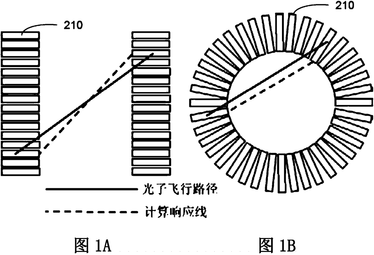
The disadvantage of coupling two photoelectric conversion devices is that the number of channels of the detector increases, resulting in a decrease in the strength of the acquired signal
Due to its own limitations, the development of software correction methods is limited

Method used


Image

  • Detector and emission imaging device having same
  • Detector and emission imaging device having same
  • Detector and emission imaging device having same

Examples


no. 1 example

[0037] Taking three layers of scintillation crystals as an example, a detector in which a row of photosensor arrays is coupled with a layer of scintillation crystals is introduced in detail.

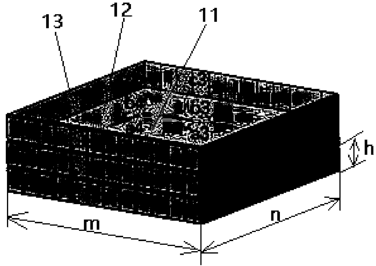
[0038] combined reference figure 2 , the detector includes three layers of scintillation crystals 11, 12, 13 and multi-row photosensor arrays a1, a2, a3, a4..., c3, c4, and the three layers of scintillation crystals are defined as 11 layers, 12 layers, 13 layers from bottom to top layer.

[0039] The size of the single-layer scintillation crystal is m×n×h (m is the length of the scintillation crystal, n is the width of the scintillation crystal, h is the height of the scintillation crystal, m>3h and n>3h), and the three-layer scintillation crystal is stacked up and down together form a multi-layer continuous crystal array, the multi-layer continuous crystal array has six faces, and the size is mⅹnⅹAh, the four faces corresponding to the size nⅹAh and mⅹAh are the side faces, and the tw...

no. 2 example

[0057] In the first embodiment, a row of photosensor arrays is shown as a detector coupled with one layer of scintillation crystals. In practical applications, the detector can also be a row of photosensor arrays coupled with two layers of scintillation crystals. A row of photosensor arrays will be described in detail below. A photosensor array is dislocation-coupled to a detector of a two-layer scintillation crystal.

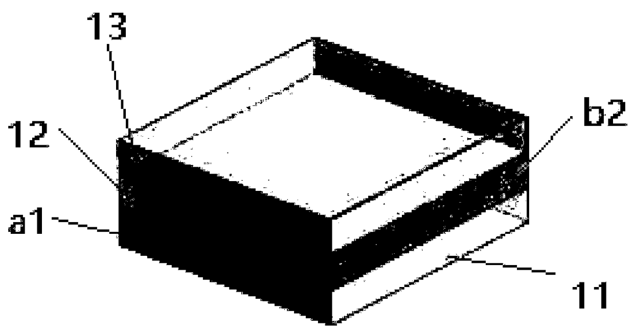
[0058] refer to Figure 4a , taking three layers of scintillation crystals as an example, the detector includes three layers of scintillation crystals 11, 12, 13 and four rows of photosensor arrays b1, b2, b3, b4, and the three layers of scintillation crystals are defined as layers 11, 12 from bottom to top layer, 13 layers.

[0059] The size of the single-layer scintillation crystal is m×n×h (m is the length of the scintillation crystal, n is the width of the scintillation crystal, h is the height of the scintillation crystal, m>3h and n>3h), and the three-la...

no. 3 example

[0075] In the second embodiment, a row of photosensor arrays is shown as a detector coupled with two layers of scintillation crystals. In practical applications, the detector can also be a row of photosensor arrays coupled with three layers of scintillation crystals. A row of photosensor arrays will be described in detail below. The photosensor array is dislocation-coupled with three layers of scintillation crystal detectors.

[0076] Such as Figure 5a and Figure 5b As shown in , it shows a detector structure of a row of optical sensor arrays coupled with a three-layer scintillation crystal, in which, Figure 5a A detector with a five-layer scintillation crystal is shown, Figure 5b Shown is a detector with eight layers of scintillation crystals. When there are five layers of scintillation crystals, the photosensor array a1 is coupled with the 11th, 12th, and 13th layers of scintillation crystals, and the photosensor array b1 is coupled with the 12th, 13th, and 14th layer...


PUM


Abstract

The invention provides a detector and an emission imaging device having the same. The detector includes multiple layers of scintillation crystals and multiple rows of optical sensor arrays. The multiple layers of scintillation crystals are stacked up and down to form a multilayer continuous crystal array. The multilayer continuous crystal array has six faces and has a size of m*n*Ah, the four faces corresponding to the sizes n*Ah and m*Ah are side faces, the two faces corresponding to the size m*n are an upper bottom surface and a lower bottom surface respectively, wherein m is the length of the scintillation crystal, n is the width of the scintillation crystal, h is the height of the scintillation crystal, and A is the number of layers of the scintillation crystals. Each row of the optical sensor arrays includes a plurality of optical sensors. The multiple rows of optical sensor arrays are coupled to the side faces of the multilayer continuous crystal array. Each row of optical sensorarrays is coupled to the side face of at least one layer of the multiple layers of scintillation crystals. The detector of the present invention has a high-performance time measurement potential.

Description

technical field [0001] The present invention relates to an emission imaging system, in particular, to a detector for an emission imaging device and an emission imaging device including the detector. Background technique [0002] Detector modules in traditional positron emission imaging systems are usually structured in upper and lower layers. The first layer is a crystal matrix composed of discrete scintillation crystals bonded together with reflective material. The five sides of the crystal matrix except the bottom are wrapped together with reflective materials. The second layer is a photoelectric sensor array, and the photoelectric sensor array is coupled with the upper surface of the crystal array. The 511keV gamma photons generated by the annihilation of positrons react in a certain crystal strip in the crystal matrix of the first layer and are converted into visible photon groups. Since the five sides of the crystal strip except the bottom surface are covered by refl...

Claims


Application Information

Patent Timeline
IPC IPC(8): G01T1/202
CPCG01T1/202
Inventor 黄秋谢思维谢杨泽翁凤花苏志宏彭旗宇
Owner DONGGUAN SONGSHAN LAKE SOUTHEN MEDICAL UNIV SCI & TECH PARK CO LTD
Learn More