Supercharge Your Innovation With Domain-Expert AI Agents!

Semiconductor device and electronic device using the same

一种半导体、电位的技术,应用在半导体器件、半导体/固态器件制造、电子开关等方向,能够解决施加等问题,达到防止错误动作或电路元件的破坏的效果

Active Publication Date: 2018-09-25
SEIKO EPSON CORP
View PDF6 Cites 0 Cited by
  • Summary
  • Abstract
  • Description
  • Claims
  • Application Information

AI Technical Summary

Problems solved by technology

However, depending on the system specification, a potential lower than the power supply potential supplied to the low potential side of the semiconductor device may be applied to the signal terminal of the semiconductor device from the outside.

Method used


Image

  • Semiconductor device and electronic device using the same
  • Semiconductor device and electronic device using the same
  • Semiconductor device and electronic device using the same

Examples


no. 1 Embodiment approach

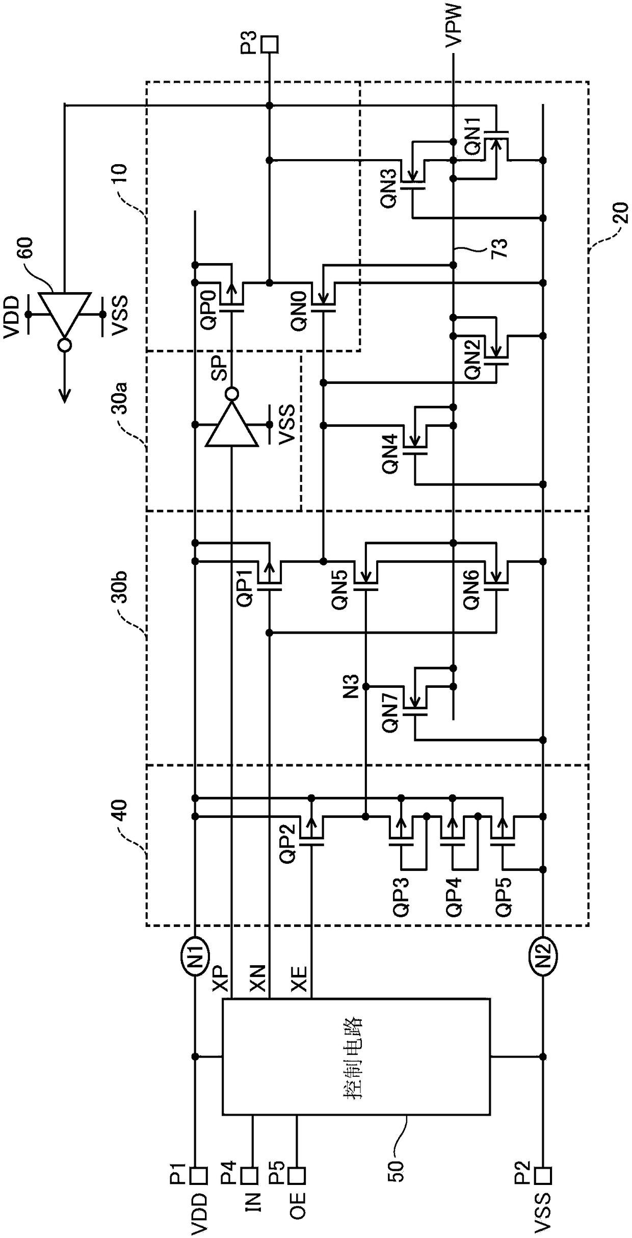
[0027] figure 1 It is a circuit diagram showing a configuration example of the semiconductor device according to the first embodiment of the present invention. like figure 1 As shown, the semiconductor device includes an output driver 10, a switch circuit 20, a high-side pre-driver 30a, a low-side pre-driver 30b, a bias potential supply circuit 40, a control circuit 50, and a plurality of terminals (pads) P1 ~P5 may also include an input circuit 60 .

[0028] The first power supply potential VDD is supplied from the power supply terminal P1 to the first node N1 of the semiconductor device. In addition, the second power supply potential VSS lower than the first power supply potential VDD is supplied from the power supply terminal P2 to the second node N2 of the semiconductor device. One of the first power supply potential VDD and the second power supply potential VSS may be the ground potential (0V).

[0029] The signal terminal P3 is at least used for outputting signals. ...

no. 2 Embodiment approach

[0068] Next, a second embodiment of the present invention will be described.

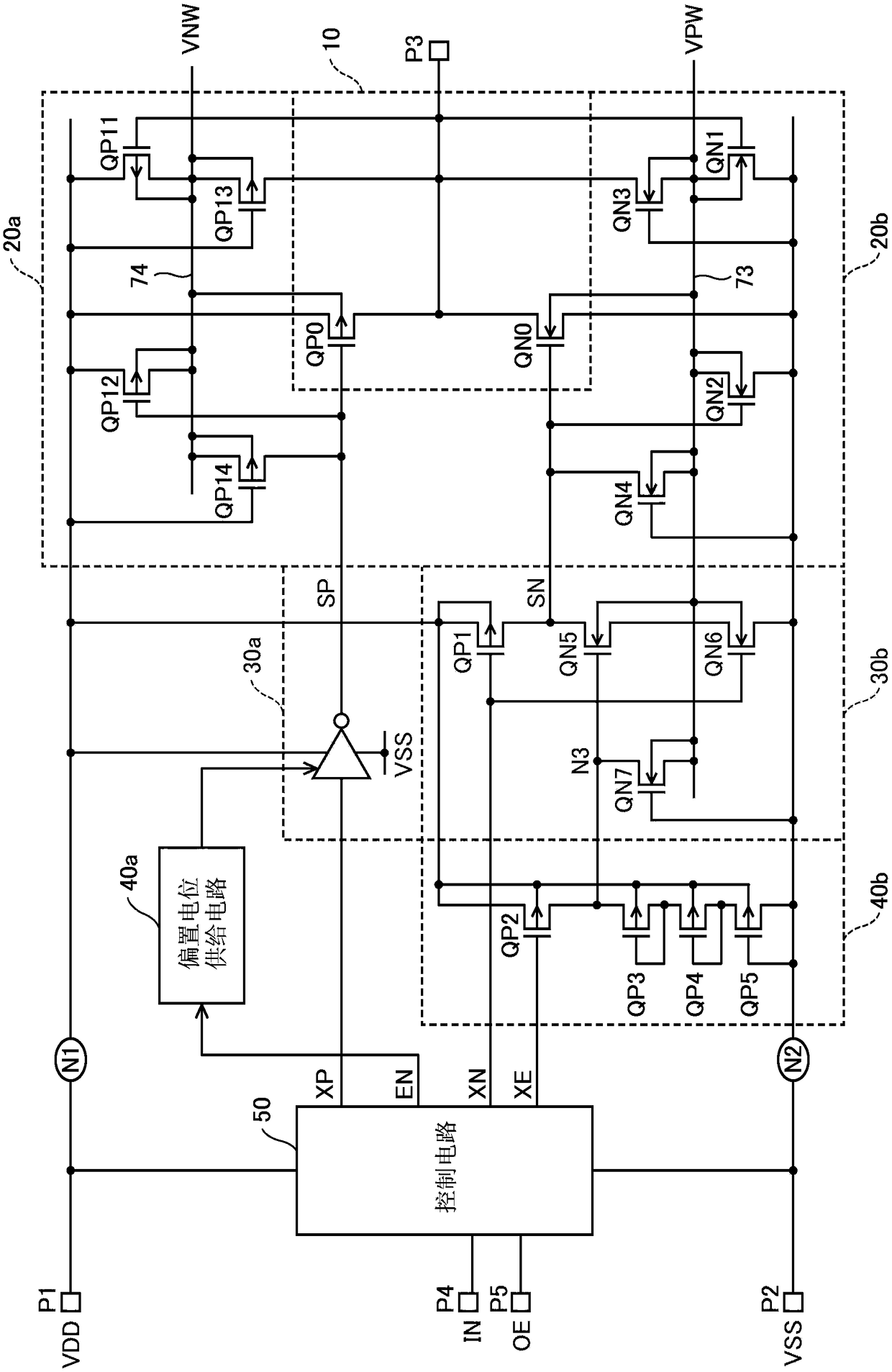
[0069] image 3 It is a circuit diagram showing a configuration example of a semiconductor device according to the second embodiment of the present invention. In the second embodiment, in the output driver 10, not only the second output element but also the first output element has the error tolerance function. In other respects, the second embodiment may be the same as the first embodiment.

[0070] like image 3 As shown, the output driver 10 includes, for example, a transistor QP0 as a first output element and a transistor QN0 as a second output element. Here, a PN junction (parasitic diode) is formed by the drain and the back gate of the transistor QP0. When the back gate of the transistor QP0 is connected to the first node N1, when a potential higher than the first power supply potential VDD and higher than the forward voltage of the parasitic diode is applied to the signal terminal P3 from...


PUM


Abstract

The invention provides a semiconductor device and an electronic device using the same. The semiconductor device is provided with a first node to which a first power supply potential is supplied, a second node to which a second power supply potential lower than the first power supply potential is supplied, a signal terminal configured to be used in order to at least output a signal, an output driver including a first output element configured to supply the first power supply potential to the signal terminal when in an ON state, and a second output element provided in a P-well electrically separated from a semiconductor substrate and configured to supply the second power supply potential to the signal terminal when in an ON state, and a switch circuit configured to selectively supply a potential to the P-well, according to at least a potential of the signal terminal.

Description

technical field [0001] The present invention relates to a semiconductor device, and more particularly, to a semiconductor device with a fault-tolerant function. Furthermore, the present invention relates to electronic equipment and the like using such a semiconductor device. Background technique [0002] For example, an external circuit that operates at a voltage higher than the power supply voltage of the semiconductor device may be connected to the signal terminal of the semiconductor device. In this case, if a leakage current flows between the external circuit and the power supply voltage of the semiconductor device fluctuates, the internal circuit may malfunction or the circuit element may be damaged. Therefore, in order to prevent leakage current, a fault tolerance function is provided in the semiconductor device. [0003] As a related art, Patent Document 1 discloses an output circuit in a semiconductor integrated circuit interfaced with a circuit operating at a volt...

Claims


Application Information

Patent Timeline
Patent Type & Authority Applications(China)
IPC IPC(8): G05F1/56
CPCG05F1/561H01L21/823892H01L27/0928H03K17/06H03K17/162H03K2017/066H03K2217/0036
Inventor 角张秀幸
Owner SEIKO EPSON CORP
Features
  • R&D
  • Intellectual Property
  • Life Sciences
  • Materials
  • Tech Scout
  • Unparalleled Data Quality
  • Higher Quality Content
  • 60% Fewer Hallucinations
Learn More