Programmable chipless electronic tag
An electronic label, chipless technology, applied to record carriers, instruments, computer parts, etc. used in machines, can solve the problems of high cost, high power consumption, large size, etc., and achieve the effect of convenience in production and use
- Summary
- Abstract
- Description
- Claims
- Application Information
AI Technical Summary
Problems solved by technology
Method used
Image
Examples
Embodiment Construction
[0020] The present invention will be further described in detail below in conjunction with specific embodiments.
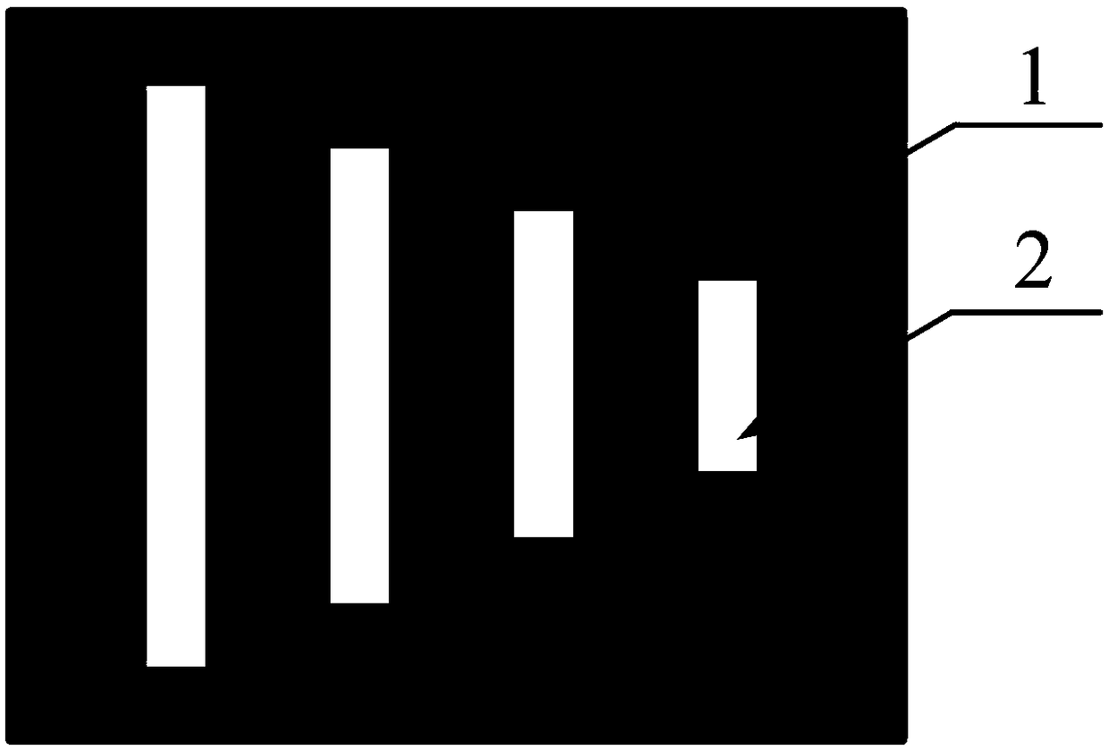
[0021] Such as figure 1 As shown, a programmable chipless electronic tag of the present invention includes a peripheral conductive area 1 and a slit pattern 2 located on the peripheral conductive area 1, wherein the peripheral conductive area 1 is a metal conductive layer deposited on an insulating substrate, so The slit pattern 2 is composed of at least one strip-shaped window, and the strip-shaped window is filled with a phase-change material capable of realizing resistance switching. In this preferred embodiment, a schematic diagram of 4-bit coding is set, such as figure 1 As shown, the phase change material is hafnium dioxide applicable to the Filament theory. The width of each strip window forming the slit pattern 2 is 1mm, and the length becomes shorter from left to right, ranging from 3mm to 50mm. Every two strips The pitch of the shaped windows is 2mm. ...
PUM
| Property | Measurement | Unit |
|---|---|---|
| Width | aaaaa | aaaaa |
| Length | aaaaa | aaaaa |
Abstract
Description
Claims
Application Information


