A wafer bonding alignment system and alignment method

A wafer bonding and alignment system technology, applied in semiconductor/solid-state device components, semiconductor devices, electrical components, etc., can solve the problem of low alignment accuracy and the inability of measurement light to reach positioning marks, wafer alignment systems and The method cannot meet the problems such as to achieve the effect of improving the wafer alignment accuracy

Active Publication Date: 2020-09-11
华天慧创科技(西安)有限公司
View PDF6 Cites 0 Cited by
  • Summary
  • Abstract
  • Description
  • Claims
  • Application Information

AI Technical Summary

Problems solved by technology

[0003] In the existing wafer bonding alignment system, when there is a certain distance between the positioning marks of the two components to be bonded, the measuring light cannot reach the positioning marks on the two components at the same time, and the alignment accuracy is low
Moreover, due to the continuous development of semiconductor technology in the direction of lightness, thinness and miniaturization, it is particularly important to achieve high-precision wafer alignment. Traditional wafer alignment systems and methods cannot meet the needs of semiconductor components with smaller feature sizes. High precision alignment requirements

Method used


Image

  • A wafer bonding alignment system and alignment method
  • A wafer bonding alignment system and alignment method
  • A wafer bonding alignment system and alignment method

Examples


Embodiment 1

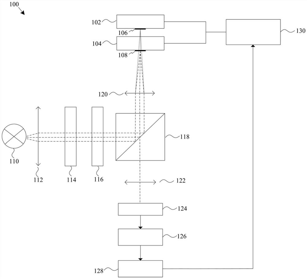
[0059] figure 1 The structure of a wafer bonding alignment system of the present invention is shown, and the wafer bonding alignment system includes:

[0060] The first wafer 102 and the second wafer 104, the first wafer is provided with a positioning mark 106, and the second wafer is provided with a positioning mark 108 corresponding to the position of the positioning mark 106, and the above two positioning marks are wafer surface plane lens;

[0061] Vision inspection system, including:

[0062] The light source 110 is used to provide measurement light, and the measurement light path is represented by a dotted line in the figure;

[0063] A collimating lens 112 configured to collimate the light emitted by the light source;

[0064] The reticle 114 is configured to superimpose a pattern on the object to be imaged, the pattern is used as a position reference, and can be aligned with the object to be imaged;

[0065] The optical retarder 116 is configured to adjust the opti...

Embodiment 2

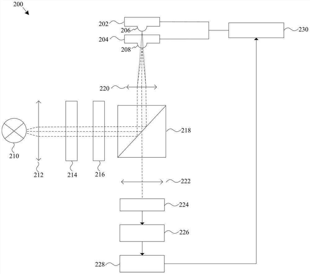
[0076] figure 2 A wafer bonding alignment system of another structure of the present invention is shown, and the wafer bonding alignment system includes:

[0077] The first wafer 202 and the second wafer 204, the first wafer is provided with a positioning mark 206, and the second wafer is provided with a positioning mark 208 corresponding to the position of the positioning mark 206, and the above two positioning marks are wafer convex lens;

[0078] Vision inspection system, including:

[0079] The light source 210 is used to provide measurement light, which is represented by a dotted line in the figure;

[0080] A collimating lens 212 configured to collimate the light emitted by the light source;

[0081] The reticle 214 is configured to superimpose a pattern on the object to be imaged, the pattern is used as a position reference, and can be aligned with the object to be imaged;

[0082] The optical retarder 216 is configured to adjust the optical path difference, so tha...

Embodiment 3

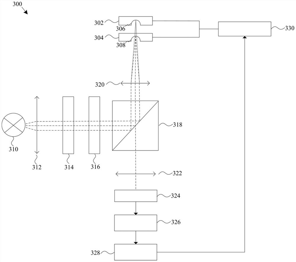
[0093] image 3 It shows a wafer bonding alignment system with another structure of the present invention. The difference between this structure and the wafer bonding alignment system shown in Embodiment 2 is that a positioning mark 306 is provided on the first wafer 302 , and the second A positioning mark 308 corresponding to the position of the positioning mark 306 is provided on the second wafer 304, and the above-mentioned two positioning marks are lenses sunken on the surface of the wafer, which are also used to verify whether the two wafers are aligned in the X and Y coordinate directions. allow.


PUM


Abstract

The invention provides a wafer bonding alignment system, which comprises a first wafer, a second wafer, a visual detection system, a driving mechanism, a controller and a computer, wherein N corresponding positioning marks are arranged on the first wafer and the second wafer respectively; and a measurement light path generated by a light source in the visual detection system is a zoom projection system, and a zoom function is achieved through an adjustable optical delay device arranged in the measurement light path. The invention further provides an alignment method based on the wafer bondingalignment system. The optical delay device is arranged in the wafer bonding alignment system, so that a defect that the reflection imaging of the positioning marks in the upper wafer and the lower wafer in a traditional wafer alignment system is not synchronous is overcome, and the voltage is modulated through the optical delay device, so that the measurement light can reach the positioning markson the two wafers almost at the same time, and imaging of images reflected from various wafer positioning marks on an image sensor can be basically synchronous, and thus the wafer alignment precisionis greatly improved, and the system and the method are suitable for a semiconductor assembly with the smaller size.

Description

technical field [0001] The invention relates to the field of wafer integration, in particular to a wafer bonding alignment system and alignment method. Background technique [0002] The existing wafer bonding alignment system and method is to set the positioning mark on the wafer, and calculate the position of the positioning mark in the wafer coordinate system by comparing the desired position and the measured value of the positioning mark in the coordinate system of the detection vision system. The position and the movement distance relative to the coordinate system of the detection vision system are used as position compensation by the data measured by the detection vision system, so that the wafers are aligned and bonded with high precision. [0003] In the existing wafer bonding alignment system, when there is a certain distance between the positioning marks of the two components to be bonded, the measuring light cannot reach the positioning marks on the two components ...

Claims


Application Information

Patent Timeline
Patent Type & Authority Patents(China)
IPC IPC(8): H01L21/68H01L23/544
CPCH01L21/681H01L23/544H01L2223/54426
Inventor 李凡月
Owner 华天慧创科技(西安)有限公司
Why Eureka
Try Eureka