Touch electrode structure and touch panel

A touch electrode and electrode layer technology, applied in the direction of electrical digital data processing, instrumentation, data processing input/output process, etc., can solve the problems of reducing touch sensitivity, increasing delay, and high connection impedance at the contact point, so as to improve touch control Sensitivity, reducing RC delay, and reducing the effect of connection impedance

Inactive Publication Date: 2018-10-12
WUHAN CHINA STAR OPTOELECTRONICS SEMICON DISPLAY TECH CO LTD
View PDF11 Cites 3 Cited by
  • Summary
  • Abstract
  • Description
  • Claims
  • Application Information

AI Technical Summary

Problems solved by technology

[0003] However, by making a touch panel with a touch electrode structure on the thin film encapsulation layer of the display panel, in order to realize the electrical connection between some electrodes, it is usually realized by building a conductive bridge; because these conductive bridges are usually s

Method used


Image

  • Touch electrode structure and touch panel
  • Touch electrode structure and touch panel
  • Touch electrode structure and touch panel

Examples


Embodiment Construction

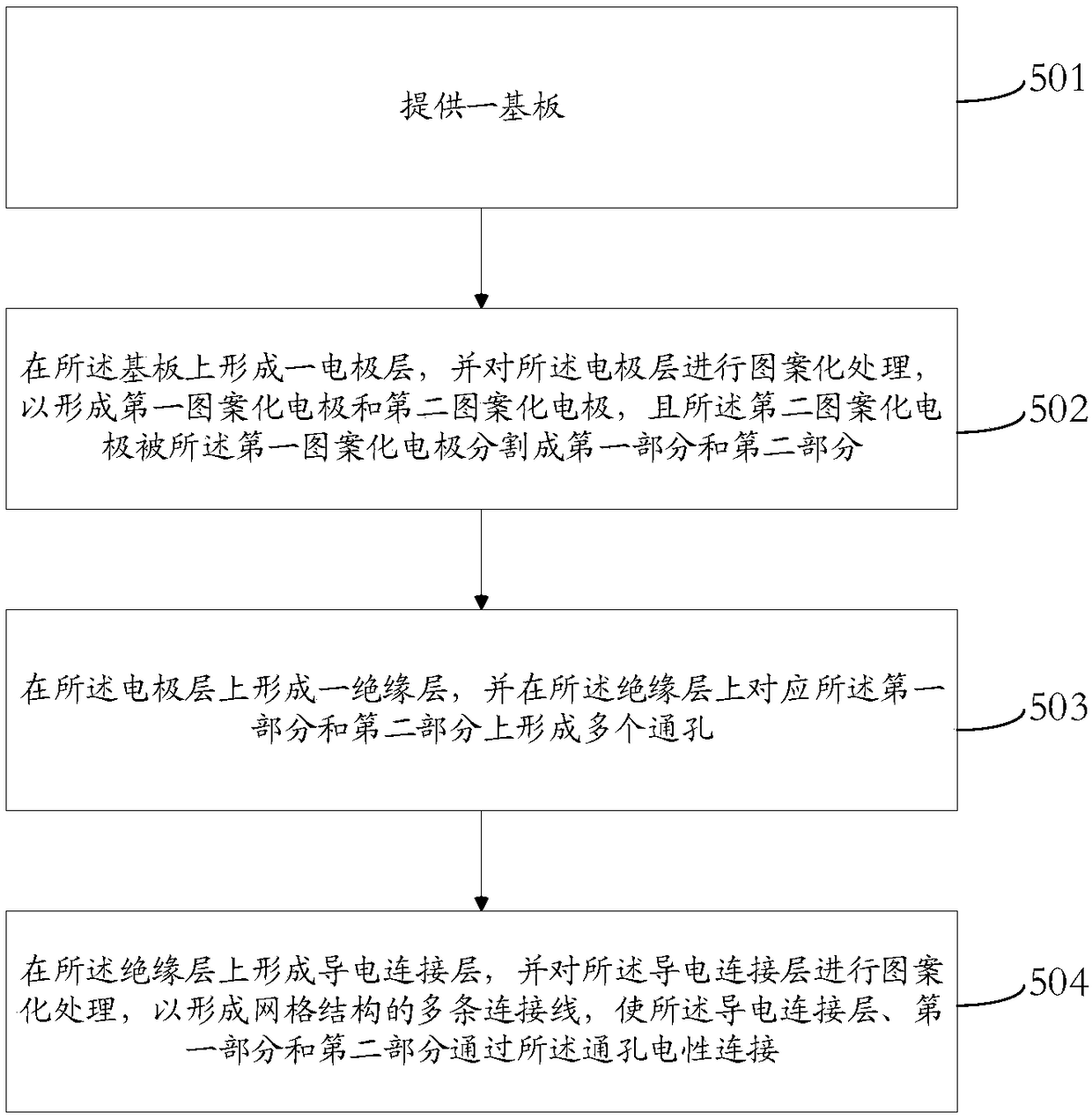
[0033] The following will clearly and completely describe the technical solutions in the embodiments of the present invention with reference to the drawings in the embodiments of the present invention. Apparently, the described embodiments are only some of the embodiments of the present invention, but not all of them. Based on the embodiments of the present invention, all other embodiments obtained by those skilled in the art without creative efforts fall within the protection scope of the present invention.

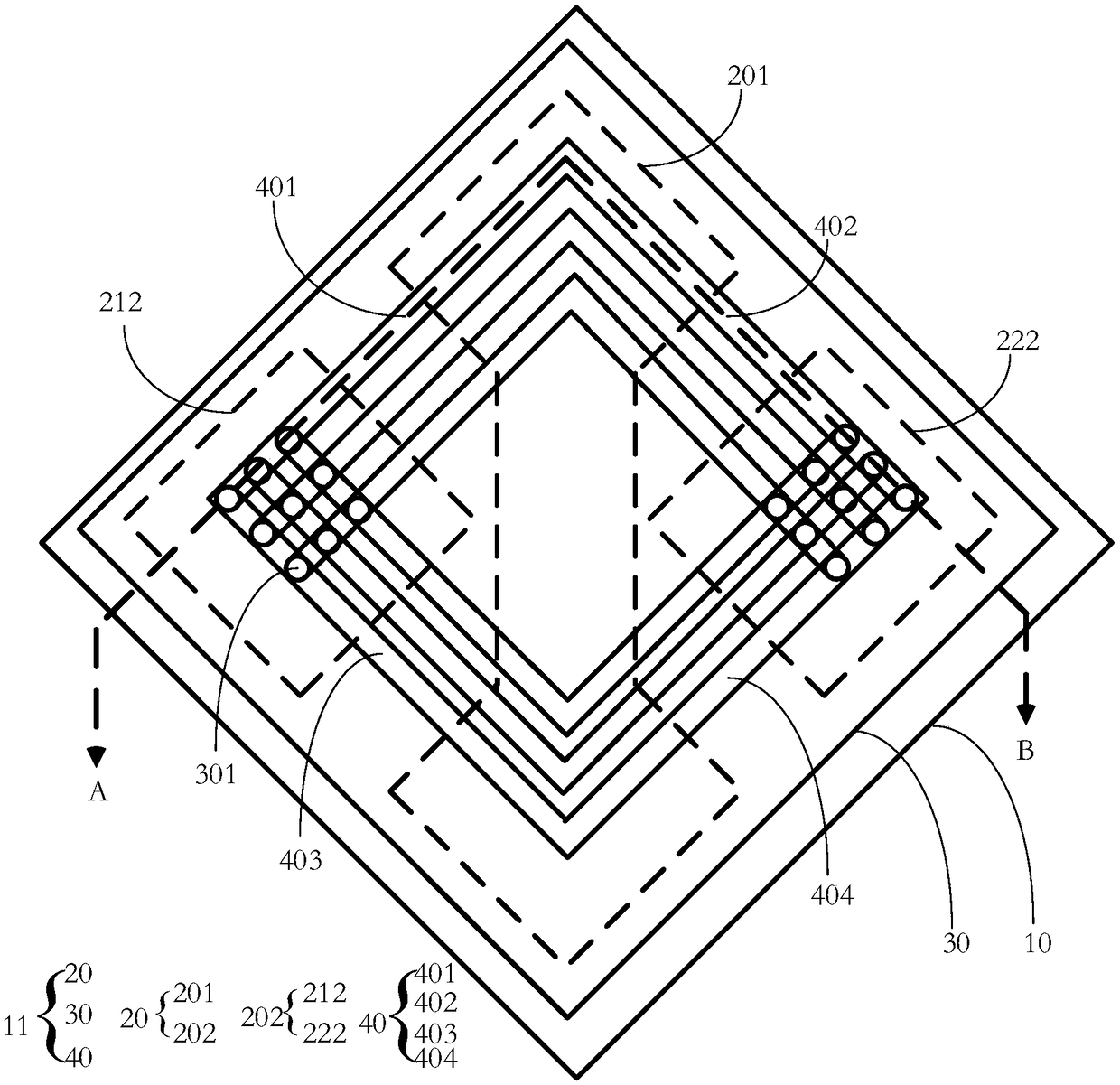
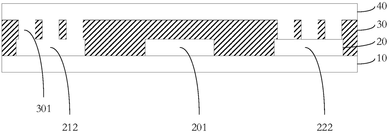
[0034] see figure 1 , figure 2 , figure 1 A planar schematic diagram of a touch electrode structure provided by an embodiment of the present invention; figure 2 for figure 1 The shown touch electrode structure is a cross-sectional view taken along the section line A-B. The touch electrode structure of the embodiment of the present invention includes a substrate 10 and a plurality of touch units 11 , and the touch units 11 are disposed on the substrate 10 .

[003...


PUM


Abstract

The invention provides a touch electrode structure and a touch panel. An insulating layer is disposed between an electrode layer and a conductive connection layer, a plurality of through holes are disposed on a corresponding first portion and second portion on the insulating layer, thus the conductive connection layer, the first portion and the second portion are enabled to be electrically connected through the through holes, thus connection resistance is lowered, then touch sensitivity is improved, RC delay is reduced, and a signal-to-noise ratio is increased.

Description

technical field [0001] The invention relates to the field of liquid crystal display, in particular to a touch electrode structure and a touch panel. Background technique [0002] With the advancement of display technology, touch technology has been widely used in various display panels. Usually, in order to realize the touch function of the display panel, one solution is to manufacture the touch panel and the display panel separately, and then attach the touch panel to the upper surface of the display panel to form a complete touch panel, but this structure will increase the touch The thickness of the control panel requires an additional bonding process; another solution is to make a touch electrode structure on the thin film packaging layer of the display panel, so as to realize the touch function of the display panel. [0003] However, by making a touch panel with a touch electrode structure on the thin film encapsulation layer of the display panel, in order to realize th...

Claims


Application Information

Patent Timeline
IPC IPC(8): G06F3/041
CPCG06F3/0416
Inventor 叶剑
Owner WUHAN CHINA STAR OPTOELECTRONICS SEMICON DISPLAY TECH CO LTD
Why Eureka
Try Eureka