Power module

a power module and power module technology, applied in the field of substrates, can solve the problems of increasing the number and integration of digital chips, increasing the space occupation and power consumption of the server, and the limitation of the individual optimization technology of components, so as to save the layout area of the system board, reduce the thickness of the substrate, and reduce the impedance of connection.

Pending Publication Date: 2022-03-10
DELTA ELECTRONICS SHANGHAI CO LTD
View PDF0 Cites 0 Cited by
  • Summary
  • Abstract
  • Description
  • Claims
  • Application Information

AI Technical Summary

Benefits of technology

[0006]An object of the present disclosure provides a substrate, a manufacturing method of the substrate and a power module with the substrate. The use of the substrate can save the layout area of the system board. Moreover, thickness of the substrate is reduced, the connection impedance is reduced, and the heat dissipation efficiency is enhanced.

Problems solved by technology

However, as the processing capacity of the server per unit volume increases, the number and the integration of the digital chips gradually increase and the space occupancy and power consumption of the server increase.
However, the technology of individually optimizing the component has limitations.
That is, it is difficult to increase the efficiency, the power density and the heat dissipating capacity of the power module.

Method used


Image

  • Power module
  • Power module
  • Power module

Examples


first embodiment

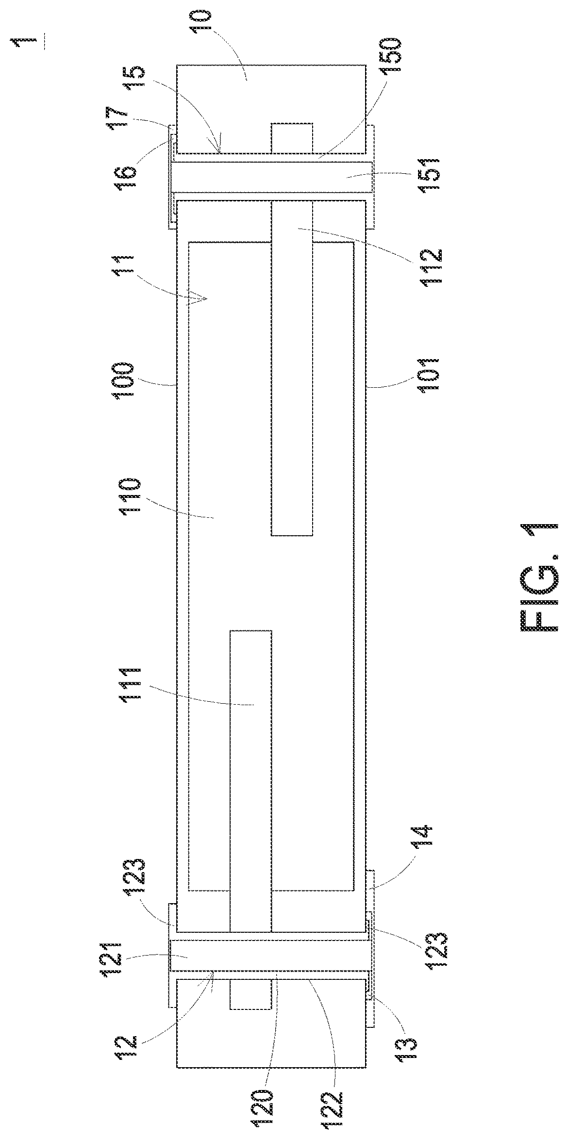
[0053]FIG. 1 is a schematic cross-sectional view illustrating a substrate according to the present disclosure. The substrate 1 includes a first insulation layer 10, at least one passive component 11, at least one first through-hole structure 12, a second insulation layer 13 and a second electrode 14. The first insulation layer 10 has a top surface 100 and a bottom surface 101. The passive component 11 is embedded in the first insulation layer 10. In the embodiment of FIG. 1, the substrate 1 includes one passive component 11. In some other embodiments, the substrate 1 includes a plurality of passive components 11. The passive component 11 includes a main body 110 and at least one first conducting terminal 111. As shown in FIG. 1, the passive component 11 further includes a second conducting terminal 112. In the embodiment of FIG. 1, the passive component 11 includes one first conducting terminal 111 and one second conducting terminal 112. In some other embodiments, the passive compon...

ninth embodiment

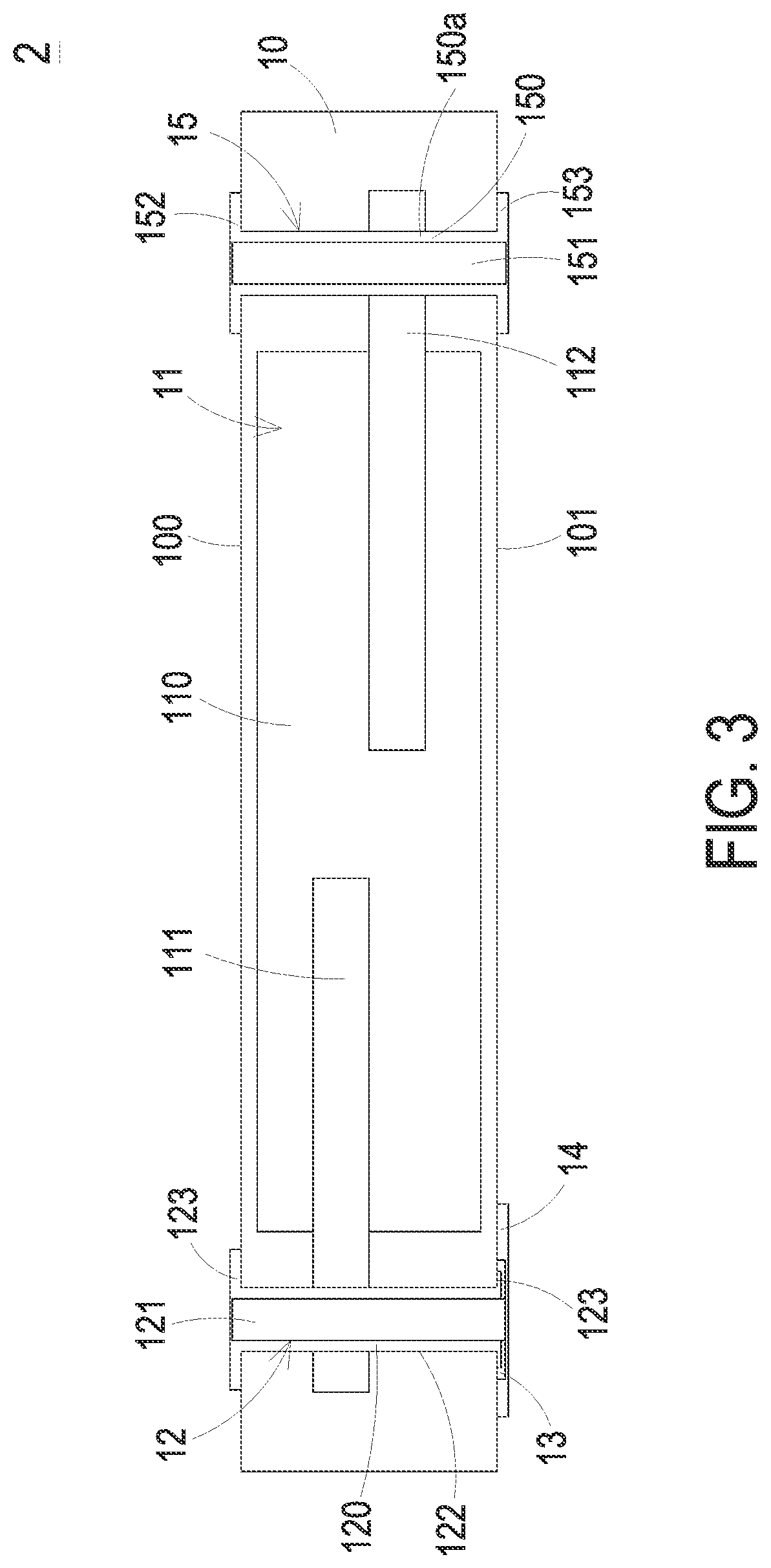
[0071]FIG. 10 is a schematic cross-sectional view illustrating a substrate according to the present disclosure. According to the practical requirements, the portion of the passive component 11 overlying the first conducting terminal 111 and the portion of the passive component 11 underlying the second conducting terminal 112 should have specified thicknesses. Therefore, the outer segment of the first conducting terminal 111 is bent in the direction toward the top surface 100 of the first insulation layer 10 and the outer segment of the second conducting terminal 112 is bent in the direction toward the bottom surface 101 of the first insulation layer 10 when compared with the embodiment of FIG. 9. Since the outer segments of the first conducting terminal 111 and the second conducting terminal 112 of the substrate 8′ of this embodiment are bent toward the top surface 100 and the bottom surface 101 of the first insulation layer 10, respectively, the current transfer path is shortened. ...

tenth embodiment

[0072]FIG. 11 is a schematic cross-sectional view illustrating a substrate according to the present disclosure. According to the practical requirements, the portion of the passive component 11 overlying the first conducting terminal 111 and the portion of the passive component 11 underlying the second conducting terminal 112 should have specified thicknesses. For shortening the current path, the structures of the first conducting terminal 111 and the second conducting terminal 112 of the substrate 9 of this embodiment are specially designed. As shown in FIG. 11, the outer segment of the first conducting terminal 111 that is located outside the main body 110 of the passive component 11 is thicker than the inner segment of the first conducting terminal 111 that is located inside the main body 110 of the passive component 11, and the outer segment of the second conducting terminal 112 that is located outside the main body 110 of the passive component 11 is thicker than the inner segmen...


PUM


Abstract

A power module includes a substrate, at least one power unit, a first carrier plate and at least one input capacitor. The power unit is disposed on the substrate and includes at least one half-bridge circuit including a first power switch and a second power switch connected in series. A second terminal of the first power switch and a first terminal of the second power switch are connected to a node. The first carrier plate and the input capacitor are arranged between the power unit and the substrate. A first electrode of the substrate is connected with the node through the first carrier plate. A top surface of a first terminal of the input capacitor is connected with a first terminal of the first power switch, and a top surface of a second terminal of the input capacitor is connected with a second terminal of the second power switch.

Description

CROSS-REFERENCE TO RELATED APPLICATION[0001]This application claims priority to China Patent Application No. 202011496240.7 filed on Dec. 17, 2020. This application is a continuation-in-part application of U.S. application Ser. No. 17 / 015,770 filed on Sep. 9, 2020 and entitled “SUBSTRATE, MANUFACTURING METHOD, AND POWER MODULE WITH SAME”, which claims priority to China Patent Application No. 201911310057.0 filed on Dec. 18, 2019. The entire contents of the above-mentioned patent applications are incorporated herein by reference for all purposes.FIELD OF THE INVENTION[0002]The present disclosure relates to a substrate, and more particularly to a substrate having a passive component embedded in an insulation layer thereof and having reduced thickness and enhanced heat dissipation efficiency. The present disclosure also relates to a manufacturing method of the substrate and a power module with the substrate.BACKGROUND OF THE INVENTION[0003]As the demands on human intelligent lives and ...

Claims


Application Information

Patent Timeline
Patent Type & Authority Applications(United States)
IPC IPC(8): H02M3/00H02M3/158H01L25/16H02M1/00
CPCH02M3/003H02M1/0064H01L25/16H02M3/158H01L25/072
Inventor HONG, SHOUYUCHEN, QINGDONGZOU, XINZHANG, MINGZHUNHUANG, JIAOPINGZHOU, JINPING
Owner DELTA ELECTRONICS SHANGHAI CO LTD
Why Eureka
Try Eureka