OLED substrate and display panel

A substrate and display area technology, applied in the direction of electrical components, electrical solid devices, circuits, etc., can solve the problems of wide panel frame and no obvious competitive advantage, and achieve the goal of increasing the overlapping area, realizing narrow frame design, and narrow frame Effect

Inactive Publication Date: 2018-10-12
BOE TECH GRP CO LTD +1
View PDF2 Cites 27 Cited by
  • Summary
  • Abstract
  • Description
  • Claims
  • Application Information

AI Technical Summary

Problems solved by technology

[0002] With the rapid development of organic display technology, the performance of organic display devices has been greatly improved, but compared with more mature liquid crystal displays (Liquid Crystal Display, LCD), organic light emitting diodes (Organic Light Emitting Diode, OLED ) The panel frame is wider, and there is no obvious competitive advantage compared with LCD products

Method used


Image

  • OLED substrate and display panel
  • OLED substrate and display panel
  • OLED substrate and display panel

Examples


no. 1 example

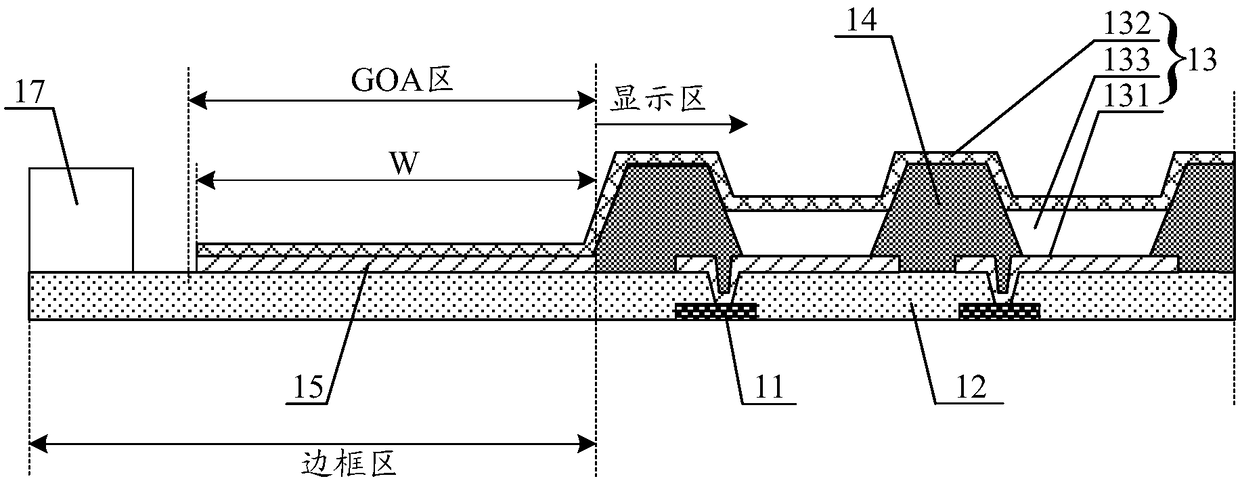
[0036] figure 2 It is a schematic structural view of the OLED substrate according to the first embodiment of the present invention. From figure 2 It can be seen from the figure that the OLED substrate includes a display area and a frame area located at the periphery of the display area. A gate driver OnArray (GOA) area of ​​the array substrate is disposed in the frame area. The OLED substrate includes a thin film transistor (Thin Film Transistor, TFT) array substrate 12 on which a plurality of TFTs 11 are arrayed. The OLED substrate also includes a plurality of OLED pixels 13 disposed on the TFT array substrate 12 . The OLED pixel area is bounded by the pixel defining layer 14 . The OLED pixel 13 includes an anode 131 , a cathode 132 and an organic light emitting layer 133 disposed between the anode 131 and the cathode 132 .

[0037] From figure 2 It can also be seen that the anode 131 is located between the pixel defining layer 14 and the TFT array substrate 12 , and...

no. 2 example

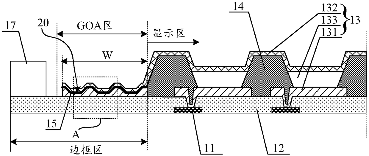
[0047] Figure 5 It is a schematic structural view of the OLED substrate according to the second embodiment of the present invention. Different from the first embodiment, in this embodiment, if Figure 5 As shown, the OLED substrate further includes a flat layer 16 disposed between the signal wiring layer 15 and the TFT array substrate 12 , and the surface of the flat layer 16 corresponding to the signal wiring layer 15 is concave-convex.

[0048] It is easy to understand that the thickness of the signal wiring layer 15 is usually relatively thin. Therefore, in order to form a bumpy overlapping surface, the thickness of the signal wiring layer 15 needs to be increased, which will lead to waste of materials. On the basis of not increasing the thickness of the signal wiring layer, the uneven overlapping surface is realized. In this embodiment, the surface of the area corresponding to the signal wiring layer 15 of the flat layer 16 is set to be uneven, In this way, when the sig...

no. 3 example

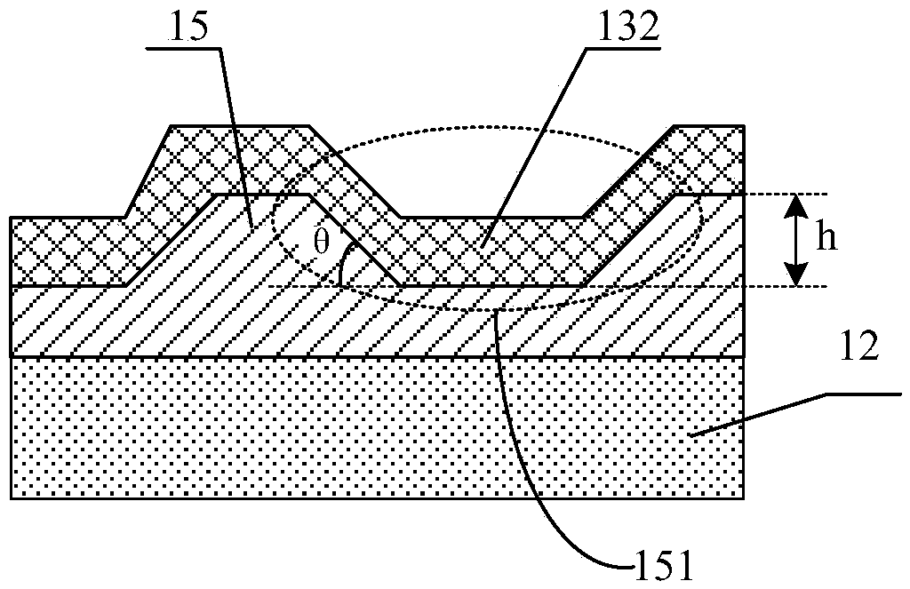
[0050] Figure 6 It is a structural schematic diagram of the overlapping surface of the cathode and the signal wiring layer according to the third embodiment of the present invention. Different from the first embodiment, in this embodiment, if Figure 6 As shown, the overlapping surface of the cathode 132 and the signal wiring layer 15 is wavy. This shape of the overlapping surface can also achieve the purpose of increasing the overlapping length of the cathode and the signal wiring layer, thereby increasing the overlapping area of ​​the cathode and the signal wiring layer, which is conducive to realizing the narrow frame of the OLED display panel.

[0051] It is easy to understand that the overlapping surface of the cathode and the signal wiring layer is not limited to the shape of trapezoidal teeth and waves, as long as the overlapping surface is concave-convex and undulating, the technical effects of the embodiments of the present invention can be achieved.

[0052] It is...


PUM


Abstract

The invention discloses an OLED substrate and a display panel. The OLED substrate comprises a display area and a GOA area located on the outer side of the display area,the GOA area is provided with asignal wiring layer,the display area is provided with an OLED pixel,a negative pole of the OLED pixel is in lap joint with the signal wiring layer,and the lap surface of the negative pole and the signal wiring layer is undulating. According to the OLED substrate,by arranging the lap surface of the negative pole and the signal wiring layer to be undulating,the lap length of the negative pole and the signal wiring layer is increased,and the lap area of the negative pole and the signal wiring layer is increased accordingly,in this way,on the basis that the lap length of the negative pole and thesignal wiring layer meets the requirement,the lap width of the negative pole and the signal wiring layer can be reduced,then the width of the GOA area is reduced,and narrow bezel design of the OLED display panel is facilitated.

Description

technical field [0001] The invention relates to the field of display technology, in particular to an OLED substrate and a display panel. Background technique [0002] With the rapid development of organic display technology, the performance of organic display devices has been greatly improved, but compared with more mature liquid crystal displays (Liquid Crystal Display, LCD), organic light emitting diodes (Organic Light Emitting Diode, OLED ) The panel frame is wider, and there is no obvious competitive advantage compared with LCD products. [0003] In order to improve the competitive advantage of OLED products, it is urgent to provide an OLED substrate to reduce the frame of the OLED display panel. Contents of the invention [0004] The purpose of the embodiments of the present invention is to provide an OLED substrate and a display panel, so as to realize a narrow frame design of the display panel. [0005] In order to solve the above technical problems, an embodiment...

Claims


Application Information

Patent Timeline
Patent Type & Authority Applications(China)
IPC IPC(8): H01L27/32
CPCH10K59/1315H10K59/131
Inventor 王建强彭利满马玲玲刘祺
Owner BOE TECH GRP CO LTD
Why Eureka
Try Eureka