LED light-emitting panel and manufacturing method thereof

A technology for light-emitting panels and manufacturing methods, applied in semiconductor/solid-state device manufacturing, electrical components, electric solid-state devices, etc., can solve problems such as unfavorable packaging reliability, LED pad damage, etc., to save solder, prevent warping, To prevent the effect of temperature difference

Active Publication Date: 2018-10-19
湖北维冠智显科技有限公司
View PDF4 Cites 2 Cited by
  • Summary
  • Abstract
  • Description
  • Claims
  • Application Information

AI Technical Summary

Problems solved by technology

[0002] Most of the existing LED packages are in the form of COB, such as attached figure 1 A plurality of LED chips 2 are mounted on the insulating substrate 1, and the LED chips 2 are flip-chip mounted on the insulating substrate 1, and then sealed with an encapsulation resin 4, and the insulating substrate 1 is drilled on the back and filled with a conductive material to form a through hole 3 In order to realize the terminal extraction of the LED chip, it needs to be drilled by laser drilling or etching, which will cause damage to the pad of the LED in the final stage, which is not conducive to the reliability of the package.

Method used


Image

  • LED light-emitting panel and manufacturing method thereof
  • LED light-emitting panel and manufacturing method thereof
  • LED light-emitting panel and manufacturing method thereof

Examples


Embodiment Construction

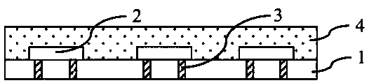
[0032] see Figure 2-8 , the manufacturing method of LED light-emitting panel of the present invention, comprises:

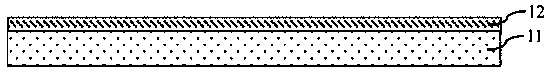
[0033] (1) Refer to figure 2 , providing a metal substrate 11, the metal substrate 11 has an opposite first surface and a second surface, and a first insulating layer 12 is formed on the first surface;

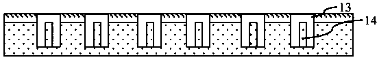
[0034] (2) Refer to image 3 , a plurality of annular blind holes 13 are formed in the metal substrate by laser slotting technology, the annular blind holes 13 penetrate the first insulating layer 12 and go deep into the metal substrate 11, the annular blind holes 13 surround A metal post 14, the first insulating layer 12 on the metal post 14 is removed at the same time;

[0035] (3) Refer to Figure 4 distributing a plurality of LED chips 15 on the first insulating layer 12 with their pads 16 facing the first insulating layer 12, the pads 16 corresponding to the annular blind holes 13 one by one, and The LED chip 15 completely covers the annular blind hol...


PUM


Abstract

The invention provides an LED light-emitting panel and a manufacturing method thereof. Blind holes are formed in advance, then the blind holes are processed into through holes, so that the damage of apad is prevented; a metal pillar with a solder layer and a dielectric layer is used as a conductive terminal, which can enhance its adhesion to a metal substrate and save solder; in addition, the metal pillar and the metal substrate are made of the same material, the temperature difference due to the difference in thermal conductivity is prevented, and warpage can be prevented.

Description

technical field [0001] The invention relates to the field of LED packaging, in particular to an LED light-emitting panel and a manufacturing method thereof. Background technique [0002] Most of the existing LED packages are in the form of COB, such as attached figure 1 A plurality of LED chips 2 are mounted on the insulating substrate 1, and the LED chips 2 are flip-chip mounted on the insulating substrate 1, and then sealed with an encapsulation resin 4, and the insulating substrate 1 is drilled on the back and filled with a conductive material to form a through hole 3 In order to realize the terminal lead-out of the LED chip, it needs to realize the drilling through laser drilling or etching process, which will cause damage to the pad of the LED in the final stage, which is not conducive to the reliability of the package. Contents of the invention [0003] Based on solving the above problems, the present invention provides a method for manufacturing an LED light-em...

Claims


Application Information

Patent Timeline
Patent Type & Authority Applications(China)
IPC IPC(8): H01L21/50H01L21/56H01L27/15
CPCH01L21/50H01L21/56H01L27/156H01L2224/18
Inventor 侯立东崔文杰
Owner 湖北维冠智显科技有限公司
Why Eureka
Try Eureka