Improved ion source cathode shield
A cathode shield and ion source technology, which is applied to solid cathodes, ion beam tubes, solid cathode components, etc., can solve problems such as shortening the service life of ion sources
Active Publication Date: 2018-10-23
AXCELIS TECHNOLOGIES
6 Cites 0 Cited by
AI-Extracted Technical Summary
Problems solved by technology
This leak shortens the life of the ion source, necessitat...
Abstract
An ion source has an arc chamber having an arc chamber body. An electrode extends into an interior region of the arc chamber body, and a cathode shield has a body that is cylindrical having an axial hole. The axial hole is configured to pass the electrode therethrough. First and second ends of the body have respective first and second gas conductance limiters. The first gas conductance limiter extends from an outer diameter of the body and has a U-shaped lip. The second gas conductance limiter has a recess for a seal to protect the seal from corrosive gases and maintain an integrity of the seal. A gas source introduces a gas to the arc chamber body. A liner has an opening configured to pass the cathode shield therethrough, where the liner has a recess.
Application Domain
Ion beam tubesSolid cathode details
Technology Topic
Electric arcEngineering +6
Image
Examples
- Experimental program(1)
Example Embodiment
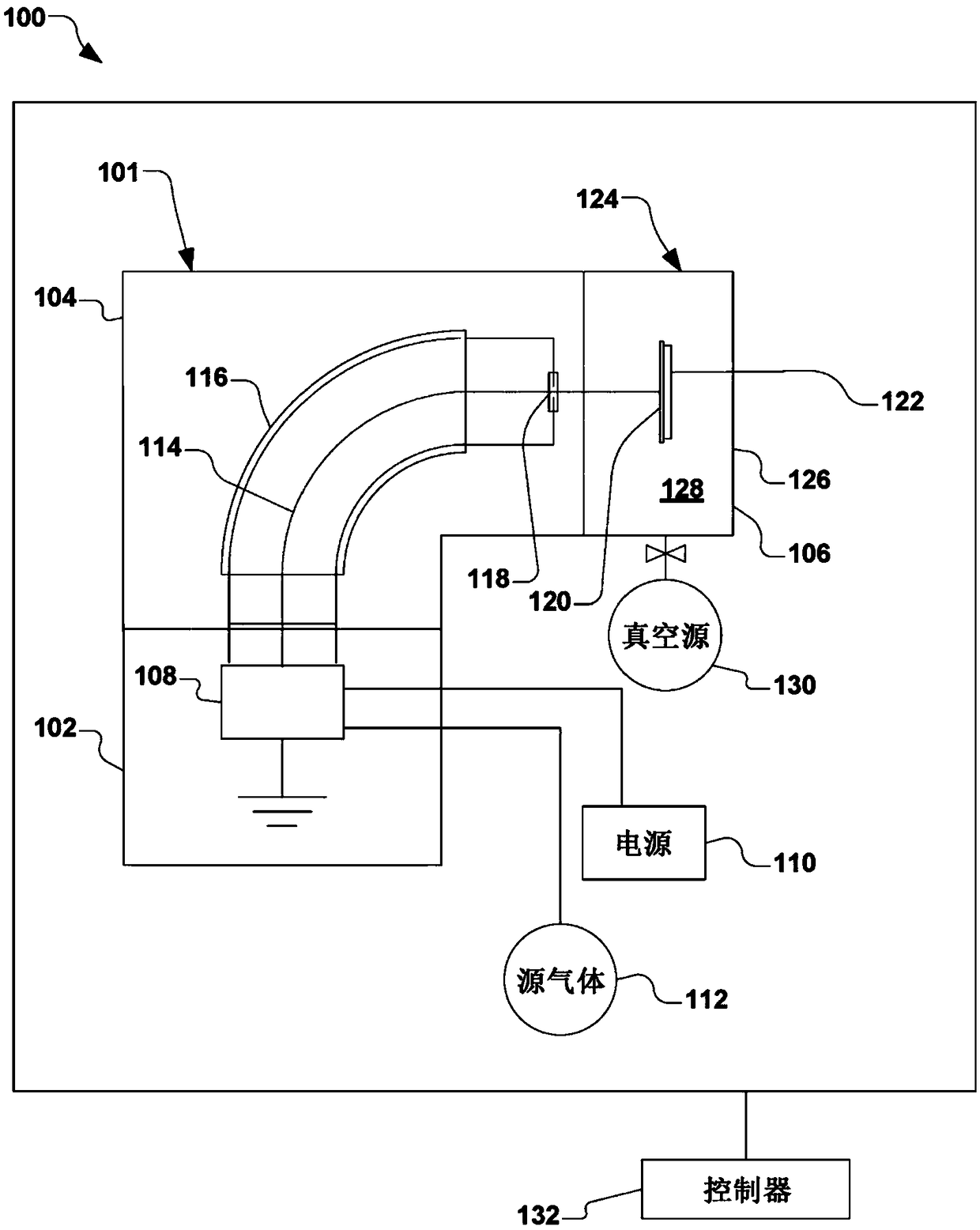
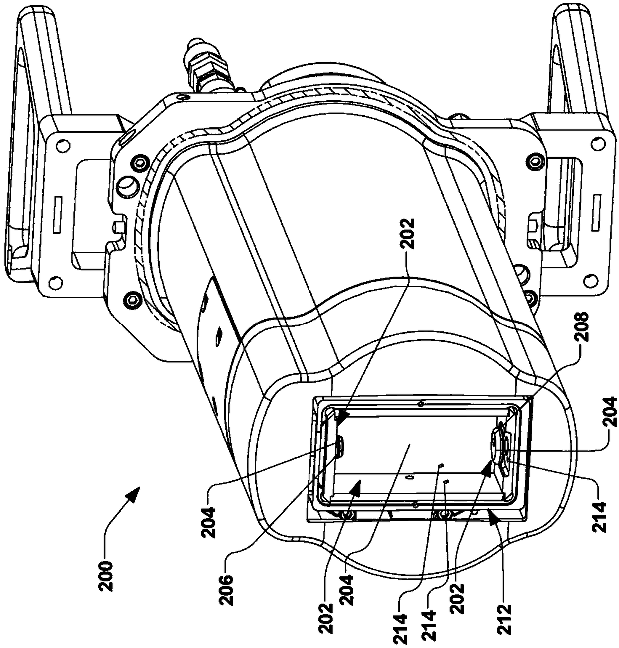
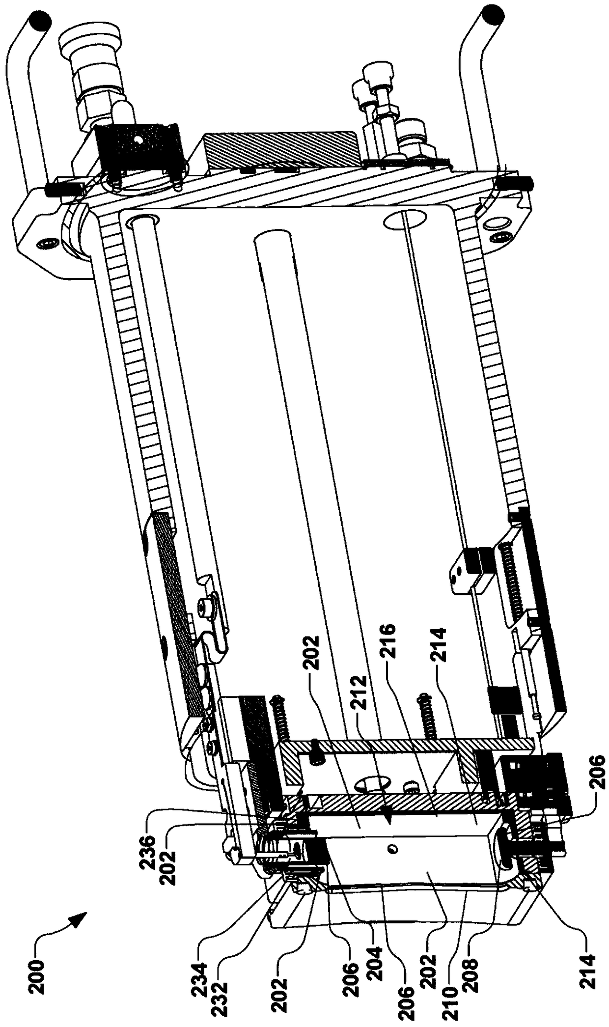
[0028] The present invention generally relates to ion implantation systems and ion sources associated therewith. More specifically, the present disclosure relates to a system and apparatus for increasing the service life of an ion source, reducing maintenance costs, and increasing the productivity of the ion source, wherein an improved cathode shield is provided for the ion source.
[0029] In view of this, the present invention will now be described with reference to the accompanying drawings, in which the same reference numerals may be used throughout the text to refer to the same elements. It should be understood that the description of these aspects is for illustrative purposes only and shall not be interpreted as limiting purposes. For explanatory purposes, several specific details are set forth below in order to fully understand the present invention. However, it will be obvious to those skilled in the art that the present invention can be implemented without these specific details. In addition, the scope of the present invention should not be limited by the embodiments or examples described below with reference to the drawings, but only by the appended claims and their equivalent changes.
[0030] It should also be noted that the drawings are used to illustrate certain aspects of the embodiments of the present invention, and therefore should be regarded as illustrative only. In particular, according to the embodiments of the present invention, the elements shown in the drawings are not necessarily drawn in proportion to each other, and the layout of each element in the drawings is selected so that the corresponding implementation can be clearly understood, and should not be understood as necessarily indicating that the implementation is The actual relative position of each component. In addition, unless otherwise specified, the features of the various embodiments and examples described herein can be combined with each other.
[0031] It should also be understood that in the following description, any direct connection or coupling between the functional modules, devices, components, circuit elements, or other physical components or functional components shown in the figures or described in the text can also be indirect connections or couplings. Followed to implement. In addition, it should also be understood that the functional modules or components shown in the figures can be implemented as individual features or components in one embodiment, and can be implemented in whole or in part as a common feature or component in another embodiment. Implement.
[0032] According to one aspect of the present invention, figure 1 An exemplary vacuum system 100 is shown. The vacuum system 100 in this embodiment includes an ion implantation system 101, but also covers other types of vacuum systems, such as plasma processing systems or other semiconductor processing systems. The ion implantation system 101 includes, for example, a terminal 102, a beam line assembly 104, and a terminal station 106.
[0033] Generally speaking, the ion source 108 in the terminal 102 is coupled to the power source 110 so that the source gas 112 (also referred to as dopant gas) supplied thereto is ionized into a plurality of ions to form an ion beam 114. In this embodiment, the ion beam 114 is guided to pass through the beam steering device 116 and pass through the perforation 118 to be directed toward the terminal station 106. In the terminal station 106, the ion beam 114 bombards a workpiece 120 (such as a silicon wafer, a display panel, etc.), and the workpiece 120 is selectively clamped or mounted to a chuck 122 (such as an electrostatic chuck or ESC). Once the implanted ions are embedded in the crystal lattice of the workpiece 120, they change the physical and/or chemical properties of the workpiece. In view of this, ion implantation is used in various applications in the manufacture of semiconductor devices, metal surface treatment, and materials science research.
[0034] The ion beam 114 of the present invention can take any form, such as a pencil beam or a spot beam, a ribbon beam, a scanning beam, or any other form that directs ions to the terminal station 106, and all of these forms fall within the scope of the present invention.
[0035] According to a typical aspect, the terminal station 106 includes a processing chamber 124, such as a vacuum chamber 126, wherein the processing environment 128 is associated with the processing chamber. The processing environment 128 is generally located within the processing chamber 124. In one example, the processing environment 128 includes a vacuum source 130 (eg, a vacuum pump) coupled to the processing chamber and configured to substantially evacuate the processing chamber. vacuum. In addition, the controller 132 is provided to control the ion implantation system 100 as a whole.
[0036] As described above, the present invention proposes a device configured to increase the utilization rate of the ion source 108 in the ion implantation system 101 and shorten its downtime. However, it should be understood that the equipment of the present invention can also be implemented in other semiconductor processing equipment, such as CVD, PVD, MOCVD, etching equipment, and various other semiconductor processing equipment, and all such embodiments should be regarded as falling into the present invention. Within the category. The device of the present invention is beneficial to prolong the use time of the ion source 108 between preventive maintenance periods, thereby improving the overall productivity and service life of the vacuum system 100.
[0037] For example, the ion source 108 (also referred to as the ion source processing chamber) can be constructed using refractory metals (tungsten (W), molybdenum (Mo), tantalum (Ta), etc.) and graphite in order to provide appropriate high temperature performance. Such materials are generally adopted by semiconductor wafer manufacturers. A source gas 112 is used in the ion source 108, wherein the source gas may or may not be conductive in nature. However, once the source gas 112 bursts or is ejected due to the fragmentation of the device, the by-products of the ionized gas may be extremely corrosive.
[0038] An example of the source gas 112 is boron trifluoride (BF 3 ), which can be used as a source gas to generate boron 11 or BF in the ion implantation system 101 2 Ion beam. At BF 3 During the ionization of molecules, three types of fluorine-containing free radicals are produced. The ion source chamber 108 can be constructed or lined with refractory metals such as molybdenum and tungsten in order to maintain its structural integrity at an operating temperature of about 700C. However, refractory fluorides are volatile and have extremely high vapor pressure even at room temperature. The fluorine base formed in the ion source chamber 108 corrodes metal tungsten (molybdenum or graphite) and forms tungsten hexafluoride (WF 6 ) (Molybdenum fluoride or carbon fluoride):
[0039] WF 6 →W + +6F - (1)
[0040] or
[0041] (MoF 6 →Mo + +6F - )(2)
[0042] Tungsten hexafluoride usually decomposes on hot surfaces. For example, in Figure 2 to Figure 3 The ion source 200 is shown in which tungsten hexafluoride or other generated materials may be decomposed on the surface 202 of the various internal components 204 of the ion source, such as the cathode 206 and the repeller 208 associated with the arc chamber 212 of the ion source And on the surface of the arc gap optics 210 (e.g. image 3 Shown). This is called the halogen cycle, as shown in equation (1), but the resulting material may also precipitate and/or condense back to the surface 202 of the arc chamber 212 in the form of contaminants 214 (eg, solid particulate contaminants or conductive films). Arc gap optics 210.
[0043] Another source of contaminants 214 deposited on the internal components comes from the cathode 206 when the cathode is heated (for example, a cathode made of tungsten or tantalum), so that the indirect heating cathode is used to start and maintain the ion source plasma (for example, Thermionic electron emission). For example, the indirect cathode 206 and the repeller 208 (for example, the opposite cathode) are at a negative potential relative to the main body 216 of the arc chamber 212, and both the cathode and the repeller can be sputtered by ionized gas. For example, the repeller 208 can be constructed of tungsten, molybdenum, or graphite. Another source of the contaminants 214 deposited on the internal components of the arc chamber 212 is the dopant material (not shown) itself. Over time, the deposited film of these contaminants 214 (for example, conductive materials) may cover the surface 202, especially the surface close to the cathode 206, thereby shortening the service life of the ion source 200.
[0044] image 3 An example of a conventional arc chamber 230 is shown in which is provided with a conventional cathode shield 232, a cathode seal 234 and a cathode liner 236. As those skilled in the art will understand with reference to the present invention, the conventional cathode shield and cathode seal The piece is intended to isolate the cathode 206 from the main body 216 of the arc chamber 212. However, with the passage of time, the use of this conventional cathode shield 232 and cathode seal 234 will generally allow ionized gas (such as fluorine or other volatile corrosive gases) to enter between the conventional cathode shield and the cathode lining 236 The gap 238 is so etched the inner diameter 240 of the cathode seal. This etching allows the ionized gas to escape and damage any nearby components, such as the insulator associated with the cathode 206. Therefore, due to etching, the service life of the ion source 200 will be shortened, and downtime associated with maintenance and/or replacement of the ion source or components can be anticipated.
[0045] According to an exemplary aspect of the present disclosure, in order to solve the problems related to such conventional devices, Figure 5 Shown in an arc chamber 300, the arc chamber is suitable for Image 6 In the ion source 301 shown, the service life of the arc chamber is greatly increased. Such as Figure 5 As shown, the arc chamber 300 includes a cathode shield 302 (sometimes called a cathode repeller), where the cathode shield includes a U-shaped lip 304, such as Figure 7A to Figure 7B Show in detail. For example, the U-shaped lip 304 is located at the end 306 of the cathode shield 302, where the U-shaped lip is usually fitted to Figure 5 In the arc chamber 300 in the arc chamber in the recess 308 (e.g., groove) in the liner 310. For example, the recess 308 in the liner 310 in the arc chamber cooperates with the U-shaped lip 304 in the cathode shield 302 to greatly reduce the gas ingress. Image 6 As shown in the conductivity of the gap 312, the gap 312 is located between the cathode shield and the through hole 314 in the arc chamber body 316 through which the cathode 318 extends.
[0046] In one example, the labyrinth seal 320 is incorporated into the outer diameter of the cathode shield 200, where the labyrinth seal is configured to receive the seal 322 (eg, a boron nitride seal). The seal 322 generally prevents Image 6 The ion source 301 in the leaks gas. In view of this, such as Figure 5 As shown, the recess 308 in the arc chamber liner 310 and the U-shaped lip 304 of the cathode shield 302 thereby protect the sealing surface 324 between the seal 322 and the arc chamber body 316 from corrosive gases, And the conductivity of corrosive gas into the gap 312 is reduced.
[0047] Although the present invention has been expressed and described in terms of one or some embodiments, it should be pointed out that the above-mentioned embodiments are only examples of certain embodiments of the present invention, and the application of the present invention is not limited by these embodiments. Especially with regard to the various functions performed by the above-mentioned components (assembly, device, circuit, etc.), unless otherwise noted, the terms used to describe these components (including the mention of "components") are intended to correspond to the implementation of the components Any component with a specific function (ie, functionally equivalent), even if it is not structurally equivalent to the structure disclosed in the exemplary embodiment of the present invention described herein. In addition, although a specific feature of the present invention is disclosed in terms of only one of the multiple embodiments, this feature can be combined with one or more other features of other embodiments if it is suitable or advantageous for any specified or specific application. In view of this, the present invention is not limited to the above-mentioned embodiments, but is intended to be limited only by the appended claims and their equivalent changes.
PUM


Description & Claims & Application Information
We can also present the details of the Description, Claims and Application information to help users get a comprehensive understanding of the technical details of the patent, such as background art, summary of invention, brief description of drawings, description of embodiments, and other original content. On the other hand, users can also determine the specific scope of protection of the technology through the list of claims; as well as understand the changes in the life cycle of the technology with the presentation of the patent timeline. Login to view more.