Photonic crystal all-optical diode

An all-optical diode and photonic crystal technology, applied in the field of optical switches, can solve the problems of difficult manufacture and complex structure, and achieve the effects of simple structure, reduced input light intensity, and widened wavelength range

Active Publication Date: 2018-11-06
SHANGHAI UNIV
View PDF6 Cites 4 Cited by
  • Summary
  • Abstract
  • Description
  • Claims
  • Application Information

AI Technical Summary

Problems solved by technology

Although the 7th-order quasi-periodic structure provided by it can realize unidirectional transmission characteristics, but the structure

Method used


Image

  • Photonic crystal all-optical diode
  • Photonic crystal all-optical diode
  • Photonic crystal all-optical diode

Examples


Embodiment 1

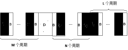
[0034] The photonic crystal all-optical diode structure of this embodiment is as attached figure 1 As shown, the period numbers of alternating high and low refractive index media on the left and right sides of the nonlinear medium D are M=6, N=8, and L=2 respectively. Medium A chooses SiO 2 Material, Refractive Index n A = 1.45, thickness d A =267.24nm; medium B chooses Bi: YIG magneto-optical material, dielectric constant ε without external magnetic field 1 =4.88, thickness d B = 175.33 nm. The dielectric layer D is a nonlinear Kerr medium with a linear refractive index n 0 =2.35, thickness d D =659.57nm, the third-order nonlinear polarization coefficient χ=1.7607×10 -11 m 2 / V 2 . The center wavelength is 1550nm.

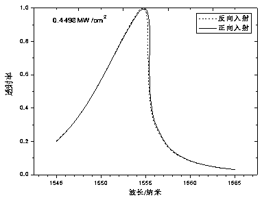
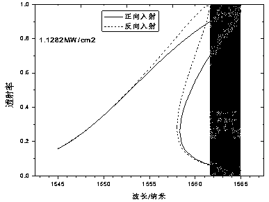
[0035] image 3 The incident light intensity is equal to 1.4820MW / cm 2 , the spectral response of the structure to normal and reverse incident light. It can be seen from the figure that this structure realizes excellent unidirectional transmission ch...


PUM


Abstract

The invention relates to a photonic crystal all-optical diode, which is formed by an asymmetrical one-dimensional photonic crystal containing a single-layer Kerr nonlinear medium. Two sides of the nonlinear medium are a regular film medium with periodic alternation and a magneto-optical medium sensitive to an external magnetic field. Based on the multivalued bistable state characteristics of a nonlinear spectral response and spatial asymmetry of the structure in the case of being larger than threshold light strength, photodiode characteristics of one-way transmission with positive incident high transmission and reverse incident cutoff can be realized. Through adjusting the size of the input light strength and/or the external magnetic field, flexible tuning of a wavelength range of an all-optical diode one-way transmission area can be realized. The all-optical diode has the protruding advantages of simple structure, easy realization, high transmission, large wavelength range, flexible tuning and the like.

Description

technical field [0001] The invention is a photonic crystal all-optical diode with flexible and adjustable characteristics, which is mainly used as an optical switch in an optical system. Background technique [0002] Since Yablonovitch and John first independently proposed the concept of photonic crystals in 1987, photonic crystals have attracted widespread attention because of their ability to control the propagation of photons. Its most important features are photonic bandgap and photonic localization. Among them, the one-dimensional photonic crystal is a dielectric structure periodically arranged in the one-dimensional space direction. It has the advantages of simple structure, excellent performance and easy integration. It is the most widely studied and practically used photonic crystal. In recent years, people have introduced photonic crystals into the field of optical communication, and designed many optical devices with excellent performance, such as photonic crystal...

Claims


Application Information

Patent Timeline
IPC IPC(8): G02B6/122G02F1/095G02F1/35G02F1/365
CPCG02B6/1225G02B2006/1213G02B2006/12145G02F1/095G02F1/3501G02F1/365
Inventor 张娟王鹏翔
Owner SHANGHAI UNIV
Why Eureka
Try Eureka